R8C/20 Group, R8C/21 Group 17. Hardware LIN
Rev.2.00 Aug 27, 2008 Page 353 of 458
REJ09B0250-0200
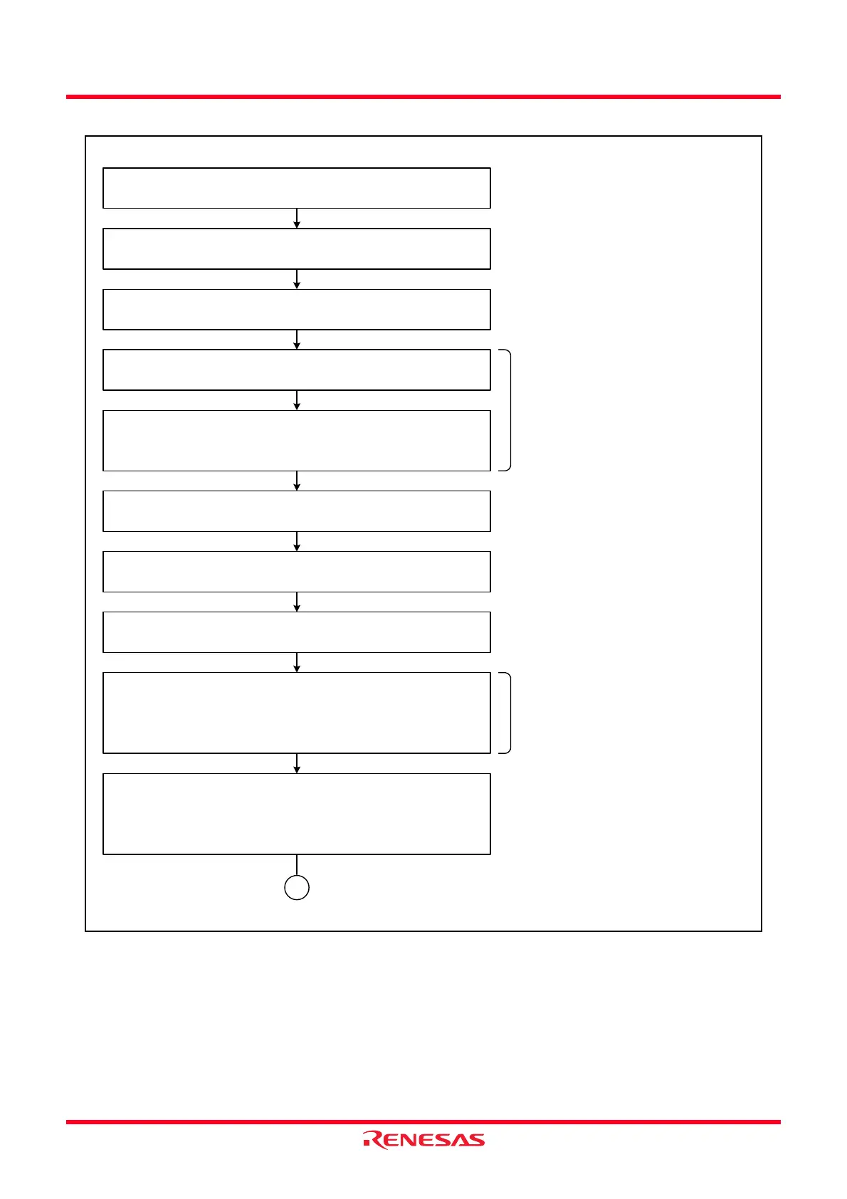
Figure 17.8 Example of Header Field Reception Flowchart (1)
Timer RA Set to pulse width measurement mode
Bits TMOD0 to TMOD2 in the TRAMR register ← 011b
Timer RA Set the pulse width measurement level low
TEDGSEL bit in the TRAIOC register ← 0
Timer RA Set the INT1/TRAIO pin to P1_5
TIOSEL bit in the TRAIOC register ← 1
Timer RA Set the count source (f1, f2, f8, fOCO)
TCK0 to 2 bits in the TRAMR register
Timer RA Set the Synch Break width
TRAPRE register
TRA register
Hardware LIN Set to slave mode
MST bit in the LINCR register ← 0
Hardware LIN Set the LIN operation to start
LINE bit in the LINCR register ← 1
Hardware LIN Set the RXD0 input unmasking timing
(After Synch Break detection, or after Synch
Field measurement)
SBE bit in the LINCR register
Hardware LIN Set the register to enable interrupts
(Bus collision detection, Synch Break
detection, Synch Field measurement)
Bits BCIE, SBIE, SFIE in the LINCR register
Set the count source and the TRA
and TRAPRE registers as suitable
for the Synch Break period.
Select the timing at which to
unmask the RXD0 input for UART0.
If the RXD0 input is chosen to be
unmasked after detection of Synch
Break, the Synch Field signal too is
input to UART0.
A
Hardware LIN Set the LIN operation to stop
LINE bit in the LINCR register ← 0
 Loading...