R8C/20 Group, R8C/21 Group 19. Flash Memory
Rev.2.00 Aug 27, 2008 Page 403 of 458
REJ09B0250-0200
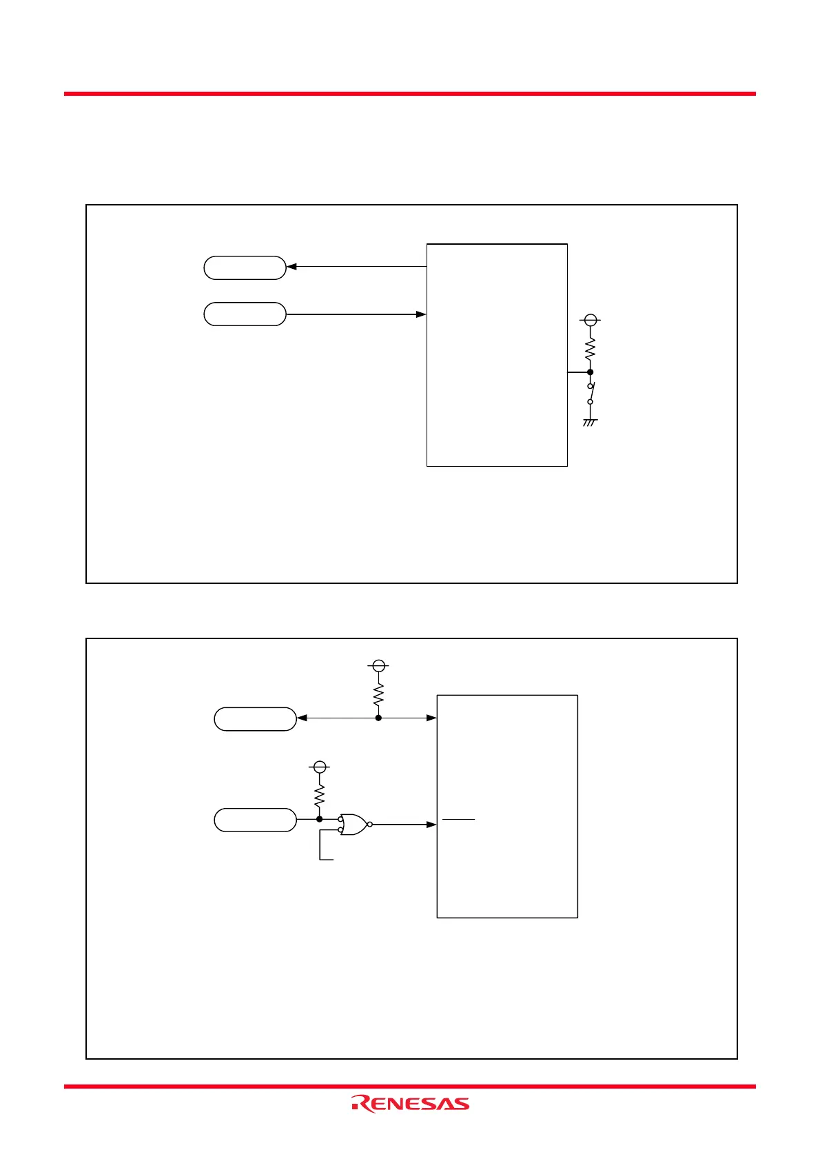
19.5.1.1 Example of Circuit Application in the Standard Serial I/O Mode
Figure 19.18 shows an example of Pin Processing in Standard Serial I/O Mode 2 and Figure 19.19 shows an
example of Pin Processing in Standard Serial I/O Mode 3. Since the controlled pins vary depending on the
programmer, refer to the manual of your serial programmer.
Figure 19.18 Pin Processing in Standard Serial I/O Mode 2
Figure 19.19 Pin Processing in Standard Serial I/O Mode 3
NOTES:
1. In this example, modes are switched between single-chip mode and
standard serial I/O mode by controlling the MODE input with a switch.
2. Connecting the oscillation is necessary. Set the main clock frequency 1
MHz to 20 MHz. Refer to Appendix Figure 2.1 Connection Example
with M16C Flash Starter (M3A-0806).
MCU
TXD
RXD
Data output
Data input
MODE
NOTES:
1.
Controlled pins and external circuits vary depending on the
programmer. Refer to the programmer manual for details.
2. In this example, modes are switched between single-chip mode and
standard serial I/O mode by connecting a programmer.
3. When operating with on-chip oscillator clock, connecting the oscillating
circuit is not necessary.
MCU
MODE
RESET
User reset signal
MODE I/O
Reset input
 Loading...