R8C/20 Group, R8C/21 Group 7. Programmable I/O Ports
Rev.2.00 Aug 27, 2008 Page 48 of 458
REJ09B0250-0200
Figure 7.9 PDi (i = 0 to 4 and 6) Registers
Figure 7.10 Pi (i = 0 to 4 and 6) Registers
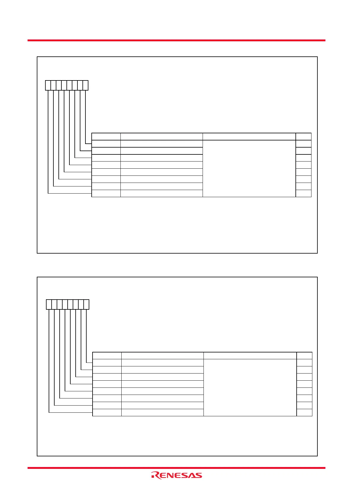
Port Pi Direction Register (i = 0 to 4, 6)
(1,2)
Symbol Address After Reset
PD0
(3)
00E2h 00h
PD1
00E3h 00h
PD2
00E6h 00h
PD3
00E7h 00h
PD4
00EAh 00h
PD6
00EEh 00h
Bit Symbol Bit Name Function RW
NOTES:
1.
2.
3.
PDi_3 Port Pi_3 direction bit
PDi_5
Port Pi_0 direction bit
Port Pi_1 direction bit
Port Pi_4 direction bit
Port Pi_2 direction bit
PDi_4
RW
RW
Port Pi_5 direction bit
RW0 : Input mode
(functions as an input port)
1 : Output mode
(functions as an output port)
RW
RW
Port Pi_6 direction bit RW
b7 b6 b5 b4 b3 b2
PDi_2
b1 b0
PDi_1
PDi_0
Write to the PD0 register w ith the next instruction after that used to set the PRC2 bit in the PRCR register to 1 (w rite
enabled).
PDi_6
RW
Nothing is assigned to the PD4_0 to PD4_2, PD4_6 and PD4_7 bits in the PD4 register.
When w riting to the PD4_0 to PD4_2, PD4_6 and PD4_7 bits in the PD4 register, w rite 0 (input mode). When read, its
content is 0.
PDi_7 Port Pi_7 direction bit RW
Nothing is assigned to the PD3_2 and PD3_6 bits in the PD3 register.
When w riting to the PD3_2 and PD3_6 bits , w rite 0 (input mode). When read, its content is 0.
Port Pi Register (i = 0 to 4, 6)
(1,2)
Symbol Address After Reset
P0
00E0h Indeterminate
P1
00E1h Indeterminate
P2
00E4h Indeterminate
P3
00E5h Indeterminate
P4
00E8h Indeterminate
P6
00ECh Indeterminate
Bit Symbol Bit Name Function RW
NOTES:
1.
2. Nothing is assigned to the P4_0 and P4_1 bits in the P4 register.
When w rite to the P4_0 and P4_1 bits, w rite 0 (“L” level). When read, its content is 0.
Nothing is assigned to the P3_2 and P3_6 bits in the P3 register.
When w riting to the P3_2 and P3_6 bits, w rite 0 (“L” level). When read, its content is 0.
Pi_7
Pi_6
RW
b3 b2 b1 b0
Pi_1
Pi_5
Pi_0
Pi_2
Pi_4
Pi_3
b7 b6 b5 b4
Por t Pi_0 bit
Por t Pi_1 bit
Por t Pi_7 bit
Por t Pi_5 bit
Por t Pi_4 bit
Por t Pi_3 bit
RW
Por t Pi_6 bit RW
Por t Pi_2 bit
RW
The pin level on any I/O port w hich is set
for input mode can be read by reading the
corresponding bit in this register. The pin
level on any I/O port w hich is set for
output mode can be controlled by w riting
to the corresponding bit in this register.
0 : “L” level
1 : “H” level
RW
RW
RW
RW
 Loading...