Home
Renesas
Control Unit
R8C/20
Renesas R8C/20 User Manual
5
of 1
of 1 rating
501 pages
Give review
Manual
Specs
To Next Page
To Next Page
To Previous Page
To Previous Page
Loading...
R8C/20 Group, R8C/21 Gro
up
7. Programmable
I/O Ports
Rev
.2.00
Aug 27, 2008
Page 47 of 458
REJ09B0250-0200
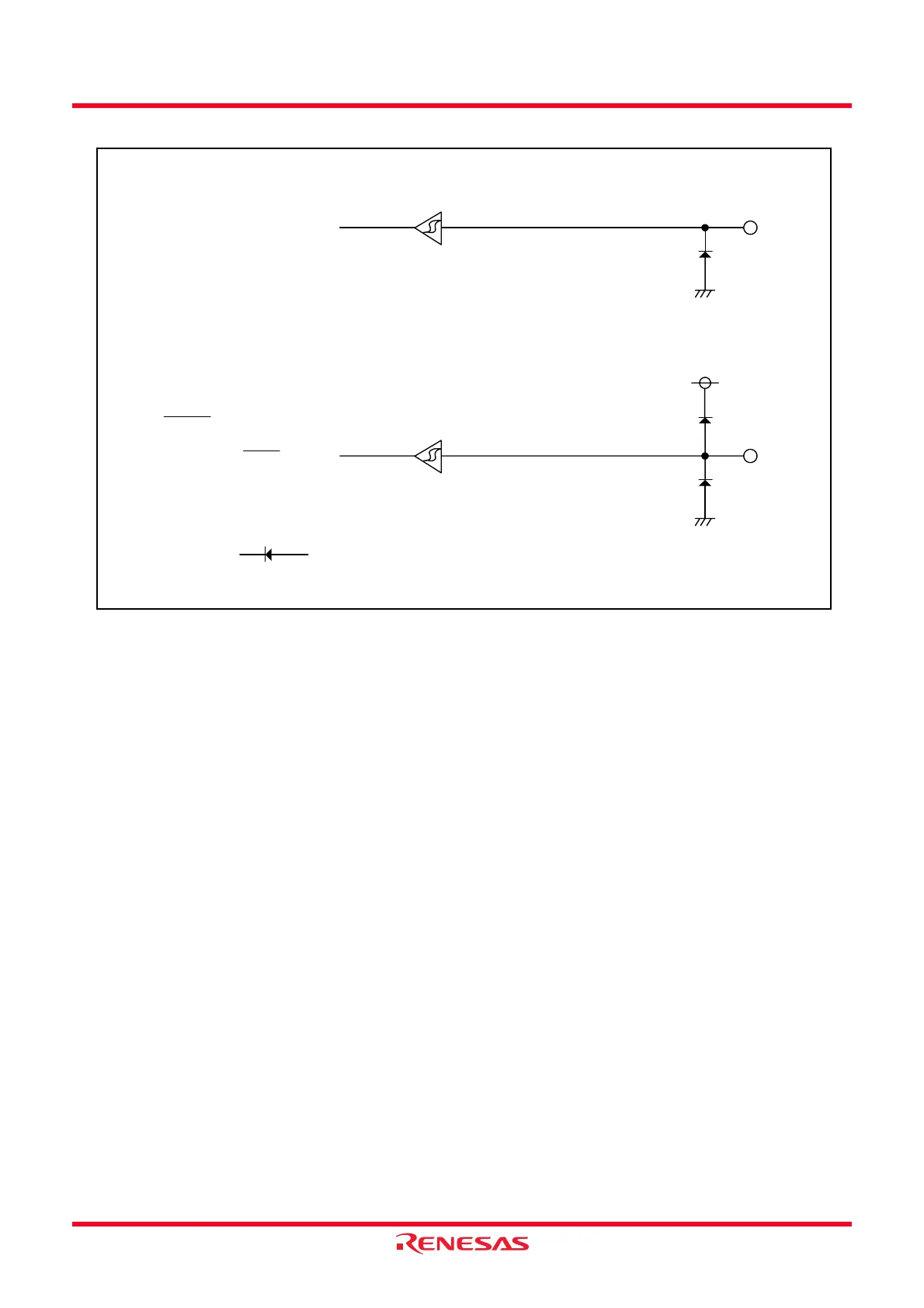
Figure 7.8
Configuration of I/O Pins
MODE
MODE signal input
RESET
RESET signal input
(1)
NOTE:
1.
symbolizes a parasitic diode.
Ensure the input voltage on each port will not exceed VCC.
(1)
62
64
Table of Contents
Default Chapter
8
Table of Contents
8
Overview
17
1 Overview
18
Performance Overview
18
Block Diagram
20
Product Information
21
Pin Assignments
23
Pin Functions
24
2 Central Processing Unit (CPU)
26
Data Registers (R0, R1, R2 and R3)
27
Interrupt Enable Flag (I)
28
3 Memory
29
R8C/21 Group
30
4 Special Function Registers (Sfrs)
31
5 Resets
37
Hardware Reset
40
Power-On Reset Function
42
Voltage Monitor 1 Reset
43
6 Voltage Detection Circuit
44
VCC Input Voltage
50
Voltage Monitor 1 Reset
51
Voltage Monitor 2 Interrupt and Voltage Monitor 2 Reset
52
7 Programmable I/O Ports
54
Effect on Peripheral Functions
55
Port Settings
66
Unassigned Pin Handling
77
8 Processor Mode
78
10 Clock Generation Circuit
80
XIN Clock
87
On-Chip Oscillator Clocks
88
CPU Clock and Peripheral Function Clock
89
Power Control
90
Wait Mode
91
Stop Mode
95
Oscillation Stop Detection Function
98
Notes on Clock Generation Circuit
101
11 Protection
102
Interrupts
103
Software Interrupts
104
Special Interrupts
105
Interrupts and Interrupt Vector
106
Interrupt Control
108
INT Interrupt
117
Inti Input Filter (I = 0 to 3)
119
Key Input Interrupt
120
Address Match Interrupt
122
Notes on Interrupts
126
Changing Interrupt Sources
127
Changing Interrupt Control Register Contents
128
13 Watchdog Timer
129
Count Source Protection Mode Disabled
132
Count Source Protection Mode Enabled
133
14 Timers
134
Timer RA
136
Timer Mode
140
Pulse Output Mode
142
Event Counter Mode
144
Pulse Width Measurement Mode
146
Pulse Period Measurement Mode
149
Notes on Timer RA
152
Timer RB
153
Timer Mode
157
Programmable Waveform Generation Mode
160
Programmable One-Shot Generation Mode
163
Programmable Wait One-Shot Generation Mode
167
Notes on Timer RB
171
Timer RD
175
Count Source
180
Buffer Operation
181
Synchronous Operation
183
Pulse Output Forced Cutoff
184
Input Capture Function
186
Output Compare Function
200
PWM Mode
216
Reset Synchronous PWM Mode
229
Complementary PWM Mode
239
PWM3 Mode
253
Timer RD Interrupt
265
Notes on Timer RD
267
Timer RE
273
Output Compare Mode
274
Notes on Timer RE
280
15 Serial Interface
281
Clock Synchronous Serial I/O Mode
287
Polarity Select Function
290
Continuous Receive Mode
291
Clock Asynchronous Serial I/O (UART) Mode
292
Bit Rate
296
Notes on Serial Interface
297
Clock Synchronous Serial Interface
298
16 Clock Synchronous Serial Interface
299
Clock Synchronous Serial I/O with Chip Select (SSU)
299
Transfer Clock
308
SS Shift Register (SSTRSR)
310
Interrupt Requests
311
Communication Modes and Pin Functions
312
Clock Synchronous Communication Mode
313
Operation in 4-Wire Bus Communication Mode
320
SCS Pin Control and Arbitration
326
Notes on Clock Synchronous Serial I/O with Chip Select
327
I 2 C Bus Interface
328
Transfer Clock
338
Interrupt Requests
339
Clock Synchronous Serial Mode
351
Noise Canceller
354
Bit Synchronization Circuit
355
Examples of Register Setting
356
17 Hardware LIN
361
Input/Output Pins
362
Register Configuration
363
Functional Description
365
Slave Mode
368
Bus Collision Detection Function
372
Hardware LIN End Processing
373
Interrupt Requests
374
Notes on Hardware LIN
375
18 A/D Converter
376
One-Shot Mode
380
Repeat Mode
383
Sample and Hold
386
A/D Conversion Cycles
387
Internal Equivalent Circuit of Analog Input
388
Output Impedance of Sensor under A/D Conversion
389
Notes on A/D Converter
390
19 Flash Memory
391
Memory Map
393
Functions to Prevent Rewriting of Flash Memory
396
ROM Code Protect Function
397
CPU Rewrite Mode
398
EW0 Mode
399
Software Commands
408
Status Registers
413
Full Status Check
414
Standard Serial I/O Mode
416
Parallel I/O Mode
420
Notes on Flash Memory
421
20 Electrical Characteristics
424
21 Usage Notes
444
Notes on Interrupts
445
Changing Interrupt Sources
446
Changing Interrupt Control Register Contents
447
Notes on Timers
448
Notes on Timer RB
449
Notes on Timer RD
453
Notes on Timer RE
459
Notes on Serial Interface
460
Clock Synchronous Serial Interface
461
Notes on Hardware LIN
462
Notes on A/D Converter
463
Notes on Flash Memory
464
Notes on Noise
467
22 Notes on On-Chip Debugger
468
23 Notes on Emulator Debugger
469
Appendix 1. Package Dimensions
470
Appendix 2. Connection Examples between Serial Writer and On-Chip Debugging Emulator
471
Appendix 3. Example of Oscillation Evaluation Circuit
472
Index
473
5
Based on 1 rating
Ask a question
Give review
Questions and Answers:
Need help?
Do you have a question about the Renesas R8C/20 and is the answer not in the manual?
Ask a question
Renesas R8C/20 Specifications
General
Brand
Renesas
Model
R8C/20
Category
Control Unit
Language
English
Related product manuals
Renesas RX110
88 pages