R8C/20 Group, R8C/21 Group 7. Programmable I/O Ports
Rev.2.00 Aug 27, 2008 Page 57 of 458
REJ09B0250-0200
X: 0 or 1
NOTES:
1. Pulled up by setting the PU07 bit in the PUR0 register to 1.
2. N-channel open drain output by setting the CSOS bit in the SSMR2 register to 1 when this pin functions as output.
X: 0 or 1
NOTES:
1. Pulled up by setting the PU07 bit in the PUR0 register to 1.
2. N-channel open drain output by setting the CSOS bit in the SSMR2 register to 1 when this pin functions as output.
X: 0 or 1
NOTE:
1. Pulled up by setting the PU07 bit in the PUR0 register to 1.
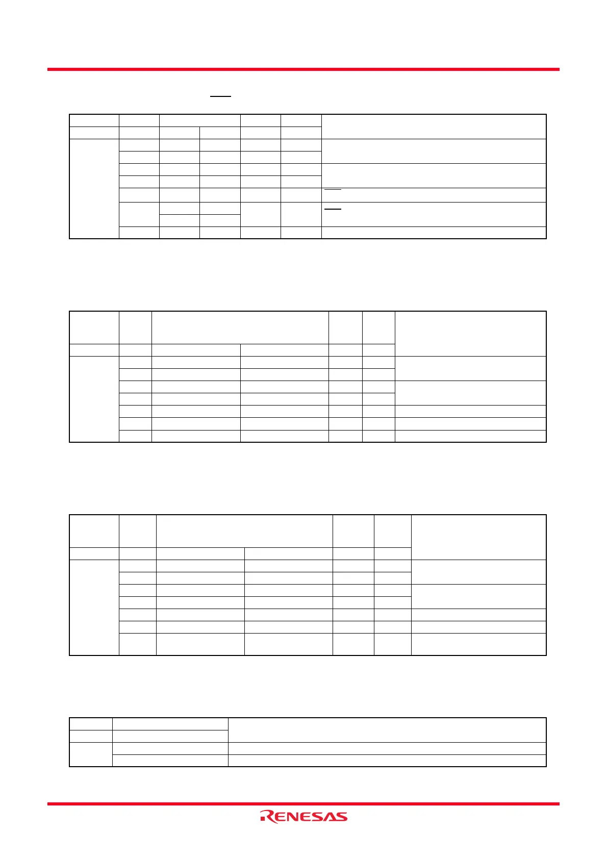
Table 7.31 Port P3_4/SDA/SCS
Register PD3 SSMR2 PMR ICCR1
Function
Bit PD3_4 CSS1 CSS0 IICSEL ICE
Setting
value
0000X
Input port
(1)
000X0
1000X
Output port
(2)
100X0
X010X
SCS
input
X
10
0X
SCS
output
(2)
11
X X X 1 1 SDA input/output
Table 7.32 Port P3_5/SCL/SSCK
Register PD3
Clock Synchronous Serial I/O with Chip Select
(Refer to Table 16.4 Association between
Communication Modes and I/O Pins.)
PMR ICCR1
Function
Bit PD3_5 SSCK output control SSCK input control IICSEL ICE
Setting
value
00 00X
Input port
(1)
00 0X0
10 00X
Output port
(2)
10 0X0
X 0 1 0 0 SSCK input
X1 000
SSCK output
(2)
X 1 0 1 1 SCL input/output
Table 7.33 Port P3_7/SSO
Register PD3
Clock Synchronous Serial I/O with Chip Select
(Refer to Table 16.4 Association between
Communication Modes and I/O Pins.)
SSMR2 PMR
Function
Bit PD3_7 SSO output control SSO input control SOOS IICSEL
Setting
value
00 0X0
Input port
(1)
0X X X1
10 0 00
Output port
1X X 01
X 0 1 0 0 SSO input
X 1 0 0 0 SSO output (CMOS output)
X1 0 10
SSO output (N-channel open-drain
output)
Table 7.34 Port P4_2/VREF
Register ADCON1
Function
Bit VCUT
Setting
value
0 Input port
1 Input port/VREF input
 Loading...