RIGOL Chapter 7 Logic Analyzer
7-8 MSO4000/DS4000 User’s Guide
4. Specify the endian
Press Endian to select “Normal” (D0 corresponds to the lowest bit of the bus
data) or “Invert” (D0 corresponds to the highest bit of the bus data). The default
is “Normal”.
5. Specify the reference clock
Press RefClock and turn the multi-function knob to select any channel of
D0 to D15 or CH1 to CH4 as the reference clock channel of BUS1. When “None”
is selected, no reference clock will be set.
1) You can set the sample edge type of the reference clock.
Press Slope to select (the rising edge) or (the falling edge).
2) When the reference clock is set to CH1 to CH4, you can set the threshold
level of the reference clock channel.
Press Threshold and turn the multi-function knob to adjust the
threshold level of the reference clock channel.
3) When the reference clock is set to “None”, you can set the on/off state of
the jitter rejection function.
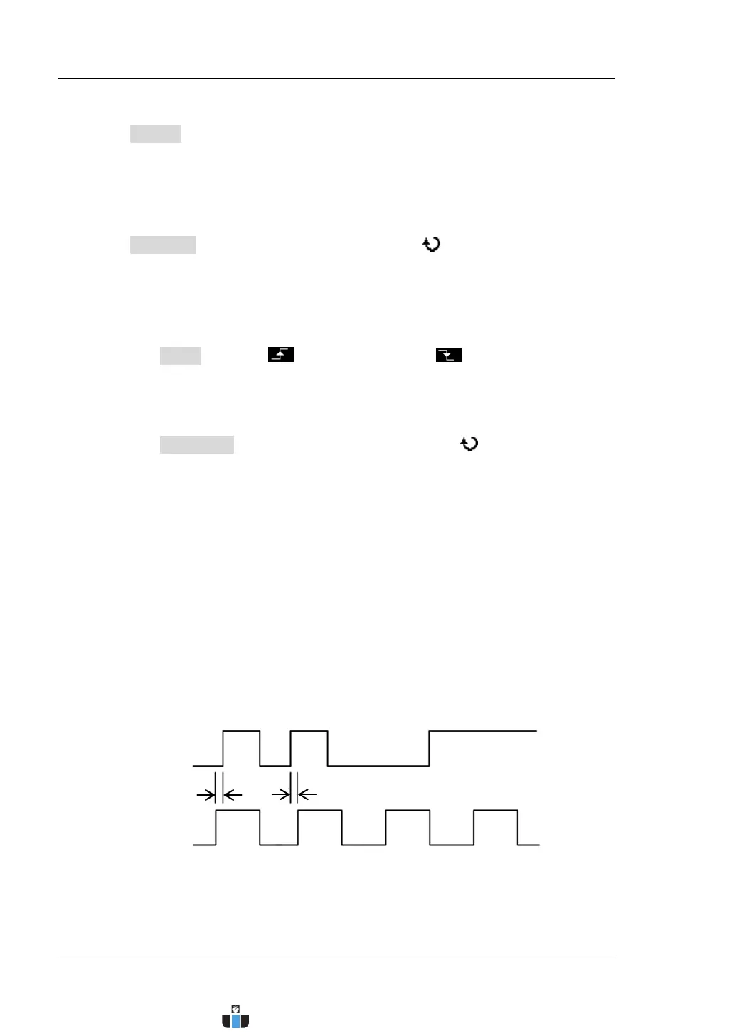
Jitter refers to the transient deviation of the signal at the specified moment
relative to its ideal time position, as shown by T1 and T2 in Figure 7-1.
When no reference clock is selected for the bus, the transition state of each
channel will lead to changes of the bus data and instable data may occur on
the bus when the channel changes. When jitter rejection is enabled, the bus
will not display the data of which the hold time is less than the “JitterTime”
and retain the previous valid data.
Figure 7-1 Digital Bus Jitter Schematic Diagram
Note: You can only set the on/off state of the jitter rejection function and
Signal
Ideal Clock
T1 T2
www.calcert.com sales@calcert.com1.800.544.2843
0
5
10
15
20
25
30