Minimum Typical Maximum
At wire cross-section 1 mm² 60 m
with a wire cross-section of 0.5 mm² 30 m
with a wire cross-section of 0.25 mm² 15 m
Cable length for power supply tolerance ± 1%
At wire cross-section 1 mm² 70 m
with a wire cross-section of 0.5 mm² 35 m
with a wire cross-section of 0.25 mm² 17 m
Input for control switch for restarting or resetting
Input resistance at HIGH 2 kΩ
Voltage for HIGH 11 V 24 V 28.8 V
Voltage for LOW –3 V 0 V 5 V
Input capacitance 15 nF
Static input current 6 mA 15 mA
Actuating time of the control switch 120 ms
EDM input
Input resistance at HIGH 2 kΩ
Voltage for HIGH 11 V 24 V 28.8 V
Voltage for LOW –3 V 0 V 5 V
Input capacitance 15 nF
Static input current 6 mA 15 mA
Response time at EDM after switching on the
O
SSDs
300 ms
Static control inputs
Input resistance at HIGH 2 kΩ
Voltage for HIGH 11 V 24 V 28.8 V
Voltage for LOW –3 V 0 V 5 V
Input capacitance 15 nF
Static input current 6 mA 15 mA
Input frequency (max. switching sequence or fre‐
q
uency)
1/t
UFVz
+ half basic response time
(t
UFVz
= time set for advancing the timing
for the switching)
OSSDs
Output signal switching device pair 2 PNP semiconductors, short-circuit pro‐
t
ected
5)
, cross-circuit monitored
Safe status when a fault occurs At least one OSSD is in the OFF state.
Switching voltage HIGH at 500 mA U
V
– 2.7 V U
V
Switching voltage LOW 0 V 0 V 3.5 V
Source switching current 6 mA 0.2 A 0.5 A
Leakage current
6)
250 µA
Load inductance
7)
2.2 H
Load capacity 2.2 µF at
50
Ω
Switching sequence (no toggling and no simulta‐
neous monitoring)
Depending on the load inductance
Permissible cable resistance
8)
2.5 Ω
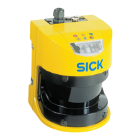
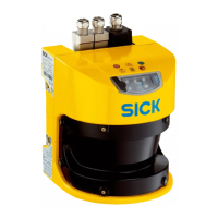
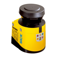
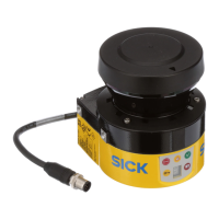
12 TECHNICAL DATA
110
O P E R A T I N G I N S T R U C T I O N S | S3000 Cold Store 8012029/ZA20/2019-11-14 | SICK
Subject to change without notice