≈ 5 ms
/15 ms
1 2 31 2 3
OSSD2
O
SSD1
120 ms/
240 ms
120 ms/
240 ms
120 ms/
240 ms
t
t
4
Figure 62: Diagram of the test pulse at the OSSDs
4
0.5 × basic response time
Approx. 5 or 15 ms
6)
af
ter the OSSDs are switched on, the device performs the first
voltage test 1 and then after a half basic response time a second voltage test 1.
After a further half basic response time of the device there is a shut-down test 2, 120
or 240 ms
6)
later a further voltage test 3. Then the device performs a shut-down test
and a voltage test alternately at an interval of 120 or 240 ms
6)
Pulse duration for the
individual tests, see figure 63, page 115, see figure 64, page 116, see figure 65,
page 116.
≈ 650 μs
< 300 μs < 300 μs
OSSD2
OSSD1
Figure 63: Voltage test after switching on the OSSDs
6)
A
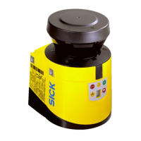
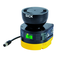
t 0.5° or 0.25° angular resolution.
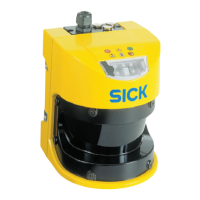
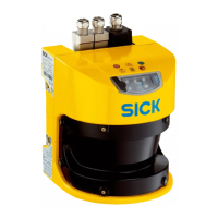
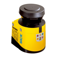
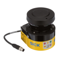
TECHNICAL DATA 12
8012029/ZA20/2019-11-14 | SICK O P E R A T I N G I N S T R U C T I O N S | S3000 Cold Store
115
Subject to change without notice