Table of contents
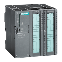
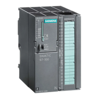
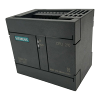
S7-300 Automation System Module data
Manual, 08/2006, A5E00105505-04
xiii
Table 3-3 Digital output modules ............................................................................................................... 3-4
Table 3-4 Digital output modules: Overview of properties (continued) ......................................................
3-4
Table 3-5 Relay output modules ................................................................................................................
3-5
Table 3-6 Digital IO modules......................................................................................................................
3-6
Table 3-7 Steps in selecting and commissioning the digital module .........................................................
3-7
Table 3-8 Parameters of SM 321; DI 16 x DC 24 V.................................................................................
3-27
Table 3-9 Assigning interrupt parameters to the inputs of SM 321; DI 16 x DC 24 V .............................
3-28
Table 3-10 Tolerances of the input delays at SM 321; DI 16 x DC 24 V ...................................................
3-28
Table 3-11 Diagnostics messages of SM 321; DI 16 x DC 24 V ...............................................................
3-29
Table 3-12 Diagnostic Messages of the SM 321; DI 16
x DC 24 V, causes of error and
troubleshooting.........................................................................................................................
3-30
Table 3-13 Dependency of input values on the CPU's operating state, and on the L+ power
supply of SM 321; DI 16
x DC 24 V ......................................................................................... 3-30
Table 3-14 Data record 0 (static parameters): ...........................................................................................
3-63
Table 3-15 Data record 1 (dynamic parameters): ......................................................................................
3-63
Table 3-16 Structure of the data record for SM 322 DO 16 x UC 24/48 V ................................................
3-64
Table 3-17 System diagnostics for SM 322 DO 16 x UC 24/48 V .............................................................
3-64
Table 3-18 Parameters of SM 322; DO 8 x DC 24 V/0.5 A........................................................................
3-77
Table 3-19 Diagnostics messages of SM 322; DO 8 x DC 24 V/0.5 A ......................................................
3-78
Table 3-20 Diagnostic messages of SM 322; DO 8
x DC 24 V/0.5 A, causes of error and
troubleshooting.........................................................................................................................
3-79
Table 3-21 Influence of the CPU operating state and of the supply voltage L+ of SM 322; DO 8
24 VDC/0.5 A on output values..............................................................................................
3-80
Table 3-22 Parameters of SM 322; DO 8 x AC 120/230 V/2 A ISOL ........................................................
3-91
Table 3-23 Diagnostic messages of SM 322; DO 8 x AC 120/230 V/2 A ISOL.........................................
3-92
Table 3-24 Diagnostic messages of SM 322; DO 8
x AC 120/230V/2 A ISOL, error causes and
troubleshooting.........................................................................................................................
3-92
Table 3-25 Parameters of SM 322; DO 8 x Rel. AC 230V/5A .................................................................
3-106
Table 3-26 Diagnostics messages of SM 322; DO 8 x Rel. AC 230V/5A................................................
3-106
Table 3-27 Diagnostic messages of SM 322; DO 8 x Rel. AC230V/5A, cause of error and
troubleshooting.......................................................................................................................
3-106
Table 3-28 Parameters of SM 327; DI 8/DO 8 x DC 24 V/0.5 A..............................................................
3-124
Table 4-1 Options of compensating the reference junction temperature.................................................
4-14
Table 4-2 Ordering data of the reference junction ...................................................................................
4-18
Table 5-1 Example: Bit pattern of a 16-bit and 13-bit analog value...........................................................
5-2
Table 5-2 Supported analog value resolutions ..........................................................................................
5-2
Table 5-3 Bipolar input ranges ...................................................................................................................
5-3
Table 5-4 Unipolar input ranges.................................................................................................................
5-3