2 Functions
274
7SA522 Manual
C53000-G1176-C155-3
R
L
the ohmic line resistance,
L
L
the line inductance.
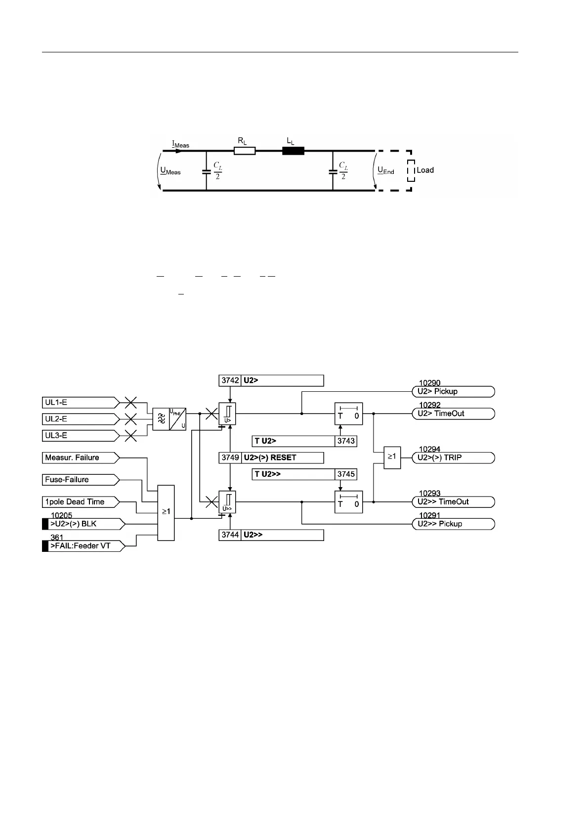
Figure 2-113 PI equivalent diagram for compounding
Overvoltage Nega-
tive Sequence
System U
2
The device calculates the negative sequence system voltages according to its defining
equation:
U
2
=
1
/
3
·(U
L1
+ a
2
·U
L2
+ a·U
L3
)
where a
= e
j120°
.
The resulting single–phase AC voltage is fed to the two threshold stages 8! and
8!!. Figure 2-114 shows the logic diagram. By combining the associated time delays
78! and 78!! a two-stage overvoltage protection for the negative sequence
system is formed. Here too, the drop-out to pick-up ratio can be set.
Figure 2-114 Logic diagram of the overvoltage protection for the negative sequence voltage system U
2
The overvoltage protection for the negative sequence system can also be blocked via
a binary input ´!8!!%/.µ. The stages of the negative sequence voltage protec-
tion are automatically blocked as soon as an asymmetrical voltage failure was detect-
ed (“Fuse–Failure–Monitor”, also see Section 2.19.1, margin heading “Fuse Failure
Monitor (Non-symmetrical Voltages)” or when the trip of the mcb for voltage transform-
ers has been signalled via the binary input ´!)$,/)HHGHU97µ (internal indication
“internal blocking”).
Even during single-pole dead time (with internal automatic reclosure function) the
stages of the negative sequence overvoltage protection are automatically blocked
since arising negative sequence values are only influenced by the asymmetrical
power flow, not by the fault in the system. If the device cooperates with an external
automatic reclosure function, or if a single-pole tripping can be triggered by a different
 Loading...