81
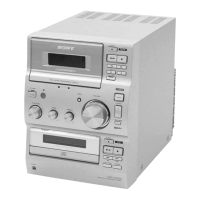
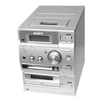
HCD-CL5MD
1 — Not used.
2 — Not used.
3 LVLI — Not used.
4 LVLO — Not used.
5 (TXD3) — Not used.
6 (RXD3) — Not used.
7 (CLK3) — Not used.
8 MUTE O Line out muting output. L: Mute
9 DARST O Reset signal output to the D/A converter. L: Active
10 SLICERSEL O IEC958 input select signal output to the D/A converter. L: CD H: MD
11 LD-LOW O Loading motor voltage control output L: High voltage H: Low voltage
12 LDIN I Loading motor control input. H: IN
13 LDOUT O Loading motor control output. H: OUT
14 MOD O Laser modulation switching signal output. L: OFF H: ON
15 BYTE I Data bus changed input. (Connected to ground.)
16 CNVSS — Ground.
17 X-CIN O Sub clock input. (32.768kHz) (Not used.)
18 X-COUT O Sub clock output. (32.768kHz) (Not used.)
19 RESET I System rest input. L : ON
20 XOUT O Main clock output. (10MHz)
21 VSS0 — Ground.
22 XIN I Main clock input. (10MHz)
23 VCC0 — Power supply. (+3.3V)
24 NMI I Fixed at H. (Pull-up)
25 DQSY I Digital in sync input. (Record system)
26 P.DOWN I Power down detection input. L: Power down
27 SQSY I ADIP (MO) sync or subcode Q (PIT) sync input from CXD2662R.(Playback system)
28 NC — Not used.
29 LDON O Laser ON/OFF control output. H: Laser ON
30 LIMIT-IN I Detection input from the limit switch. L: Sled limit-In H: Sled limit-Out
31 C2-PWM-B — Not used.
32 XINIT I Interrupt status input from CXD2662R.
33 — Not used.
34 XELT I XELT input from DSP IC.
35 WR PWR O Write power ON/OFF output. L: OFF H: ON
36 IIC CLK I/O IIC serial clock input/output.
37 IIC DATA I/O IIC serial data input/output.
38 SWDT O Writing data signal output to the serial bus.
39 VCC1 — Power supply. (+3.3V)
40 SRDT I Reading data signal input from the serial bus.
41 VSS1 — Ground.
42 SCLK O Clock signal output to the serial bus.
43 REC-SW I Detection signal input from the recording position detection switch. L: REC
44 CLIP DTO O CLIP serial data output.
45 CLIPDTI I CLIP serial data input. (Not used.)
46 CLIP CLK O CLIP serial clock output. (Not used.)
47 DIG-RST O Digital rest signal output to the CXD2662R and motor driver. L: Reset
48 SENS I Internal status (SENSE) input from the CXD2662R.
49 PLAY-SW I Detection signal input from the playback position detection switch. L: PLAY
50 XLAT O Latch signal output to DSP IC.
51 OUT-SW I Detection signal input from the loading out detection switch.
52 — Not used.
FunctionPin Name
Pin No.
I/O
• IC1001 M30805MG-205GP SYSTEM CONTROL (DIGITAL BOARD)