82
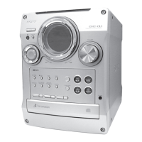
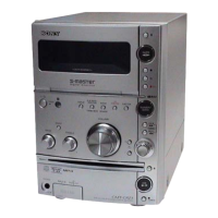
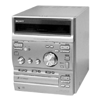
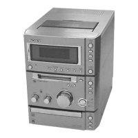
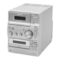
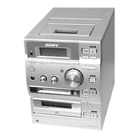
HCD-CL5MD
53 — Not used.
54 — Not used.
55 O Not used.
56 MNT2 (XBUSY) I In the state of executive command from the CXD2662R
57 VSS2 — Ground.
58 MNT1 (SHCK) I Track jump signal input from the CXD2662R
59 VCC2 — Power supply. (+3.3V)
60 EEP-WP O EEP-ROM write protect signal output. L: write possibility
61 SDA (EEP) I/O Data signal input/output pin with the EEP-ROM.
62 BCLK/ALE/CLKO — Not used.
63 RD/DW O Read signal output.
64 BHE/CASH — Not used.
65 WR/CASL O Write signal output.
66 SCL O Clock signal output to the EEP-ROM.
67 REFLECT I Disk reflection rate detection input from the reflect detection switch. H: Disk with low reflection rate
68 PROTECT I Recording-protection claw detection input from the protection detection switch. H: Protect
69 CS0 O Chip select signal output to the Flash ROM.
70 CS1 O Not used.
71 O Not used.
72 A20 O Address bus signal output to Flash ROM.
73 A19 O Address bus signal output to Flash ROM.
74 VCC3 — Power supply. (+3.3V)
75 A18 O Address bus signal output to Flash ROM.
76 VSS3 — Ground
77 to 85 A17 to A9 O Address bus signal output to Flash ROM.
86 to 89 SEL 3 to 0 O Not used.
90 WP O Write protect signal to the Flash ROM.
91 VCC4 — Power supply. (+3.3V)
92 A8 O Address bus signal output to Flash ROM.
93 VSS4 — Ground.
94 to 100 A7 to A1 O Address bus signal output to Flash ROM.
101 LB — Not used.
102 to 113 D15 to D4 I/O Data bus signal input/output to the Flash ROM.
114 CLIP-SEL O Not used.
115 IIC BUSY O IIC cable connect check. L: Active
116 DALOCK O LOCK signal input from D/A converter.
117 LINE-MUTE O Not used.
118 ADP DOWN O Reset signal output to the A/D converter.
119 to 122 D3 to D0 I/O Data bus signal input/output to the Flash ROM.
123 SPDIF-CUT — Jog dial pulse input from the rotary encoder.
124 OPT SEL O Optical select signal output.
125 to 129 — Not used.
130 VSS5 — Ground.
131 O Not used.
132 VCC5 — Power supply. (+3.3V)
133 OP-LEVEL I Optical Pick-up voltage (current) detect signal input.
134 to 139 — Not used.
140 AVSS — Ground. (Analog)
141 — Not used.
142 VREF — Power supply. (+3.3V)
143 AVCC — Power supply. (+3.3V)
144 NC I Not used.
FunctionPin NamePin No. I/O