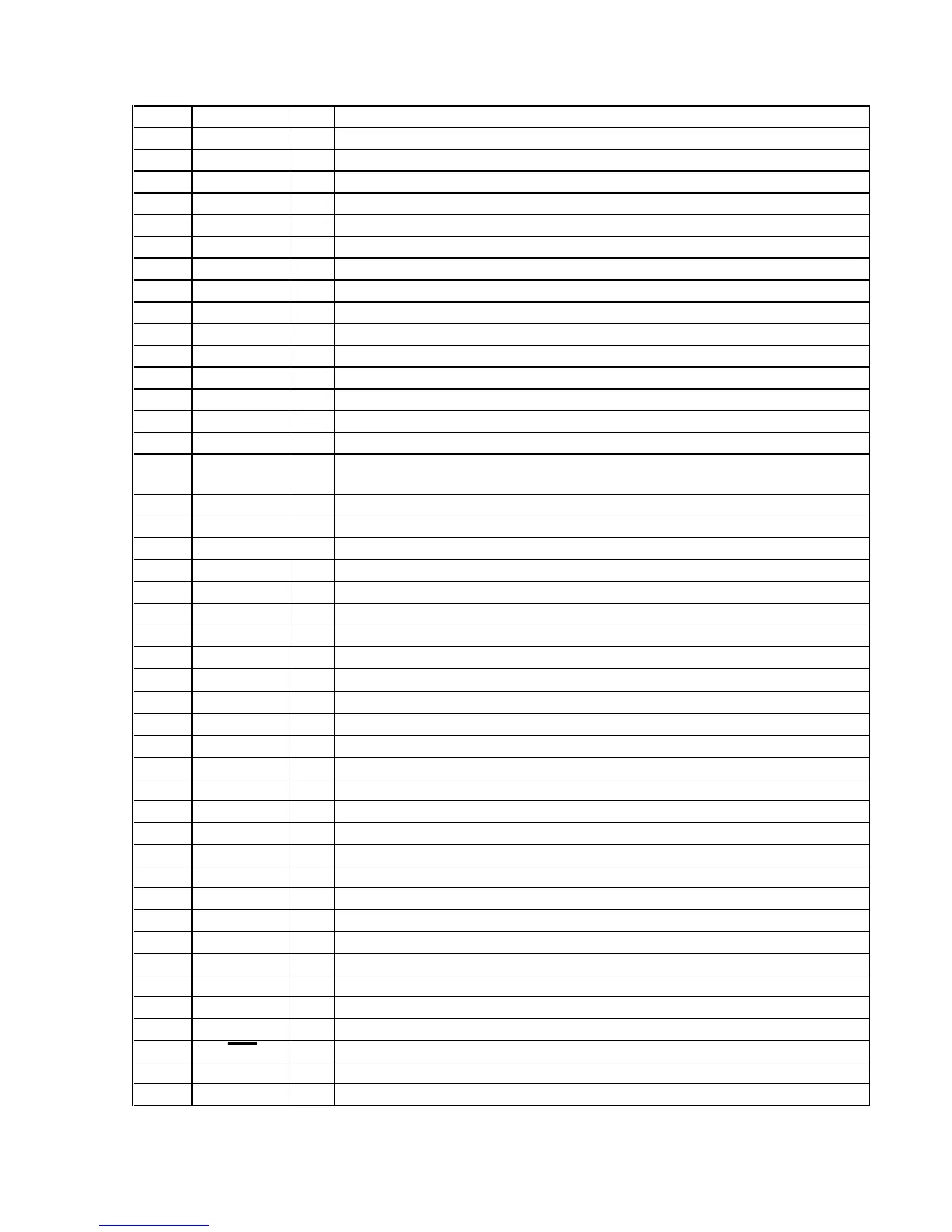
109
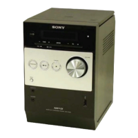
HCD-FL5D
Pin No. Pin Name I/O Description
48
VSS —
Ground terminal
49
WMD0 I
S-RAM wait mode setting terminal Fixed at “L” in this set
50
PAGE2 O
Page selection signal output terminal Not used
51
VSS —
Ground terminal
52, 53
PAGE1, PAGE0 O
Page selection signal output terminal Not used
54
BOOT I
Boot mode control signal input terminal Not used
55
BTACT O
Boot mode state display signal output terminal Not used
56
BST I
Boot trap signal input from the digital audio interface receiver
57
MOD1 I
PLL input frequency select terminal “L”: 384fs, “H”: 256fs (fixed at “H” in this set)
58
MOD0 I
Mode setting terminal “L”: single chip mode, “H”: use prohibition (fixed at “L” in this set)
59
EXLOCK I
PLL lock error and data error flag input from the digital audio interface receiver
60
VDDI —
Power supply terminal (+3.3V)
61
VSS —
Ground terminal
62, 63
A17, A16 O
Address signal output terminal Not used
64 to 66
A15 to A13 O
Address signal output to the S-RAM
67
GP10 O
L/R sampling clock signal (44.1 kHz) output to the D/A, A/D converter (IC605) and digital filter
Not used
68
DECODE O
Decode signal output to the system controller
69
AUDIO I
Bit 1 input terminal of channel status from the digital audio interface receiver
70
VDDI —
Power supply terminal (+3.3V)
71
VSS —
Ground terminal
72 to 75
D15 to D12 I/O
Two-way data bus with the S-RAM
76
VDDE —
Power supply terminal (+3.3V)
77 to 80
D11 to D8 I/O
Two-way data bus with the S-RAM
81
VSS —
Ground terminal
82 to 85
A9, A12 to A10 O
Address signal output to the S-RAM
86
TDO O
Simple emulation data output terminal Not used
87
TMS I
Simple emulation data input start/end detection signal input terminal Not used
88
XTRST I
Simple emulation asychronous break input terminal Not used
89
TCK I
Simple emulation clock signal input terminal Not used
90
TDI I
Simple emulation data input terminal Not used
91
VSS —
Ground terminal
92 to 97
A8 to A3 O
Address signal output to the S-RAM
98, 99
D7, D6 I/O
Two-way data bus with the S-RAM
100
VDDI —
Power supply terminal (+3.3V)
101
VSS —
Ground terminal
102 to 105 D5 to D2 I/O
Two-way data bus with the S-RAM
106
VDDE —
Power supply terminal (+3.3V)
107, 108
D1, D0 I/O
Two-way data bus with the S-RAM
109, 110
A2, A1 O
Address signal output to the S-RAM
111
VSS —
Ground terminal
112
A0 O
Address signal output to the S-RAM
113
PM I
PLL reset signal input from the digital audio interface receiver
114
SDI3 I
Audio serial data input terminal Not used
115
SDI4 I
Audio serial data input terminal Not used