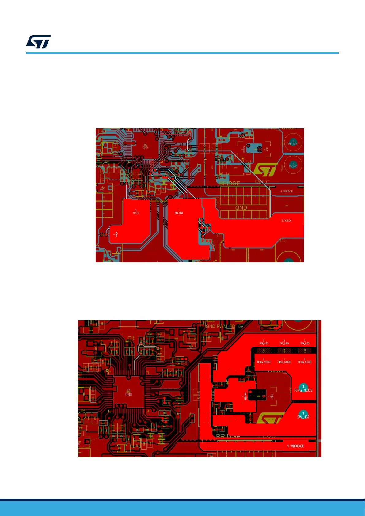
7.2.6 DC-DC boost circuit
The DC-DC boost circuit is placed close to the input of the board to minimize the current loops. Q300 and Q301
MOSFETs are placed close to L300 for the same reason. The tracks connecting R300 to the input and to L300
are wide to accommodate for the input current.
The circuit is also placed close to STWBC2 to reduce the gate driver and sensing tracks length.
The GND terminals of the capacitors are connected to other GND planes using multiple vias.
Figure 54. DC-DC boost circuit routing
7.2.7 Main bridge circuit
The bridge circuit is placed close to the output of the DC-DC boost circuit. Large polygons are used for the
Vbridge, Ring node and MOSFET tracks to accommodate for high currents. The GND terminals of the sensing
resistor and the Vbridge capacitors are grounded to the other ground planes through multiple vias.
Figure 55. Main bridge circuit
UM3286
Designing a wireless power transmitter based on STEVAL-WBC2TX70 evaluation board
UM3286 - Rev 1
page 70/84