4 Device description and operation
4.1 System block diagram
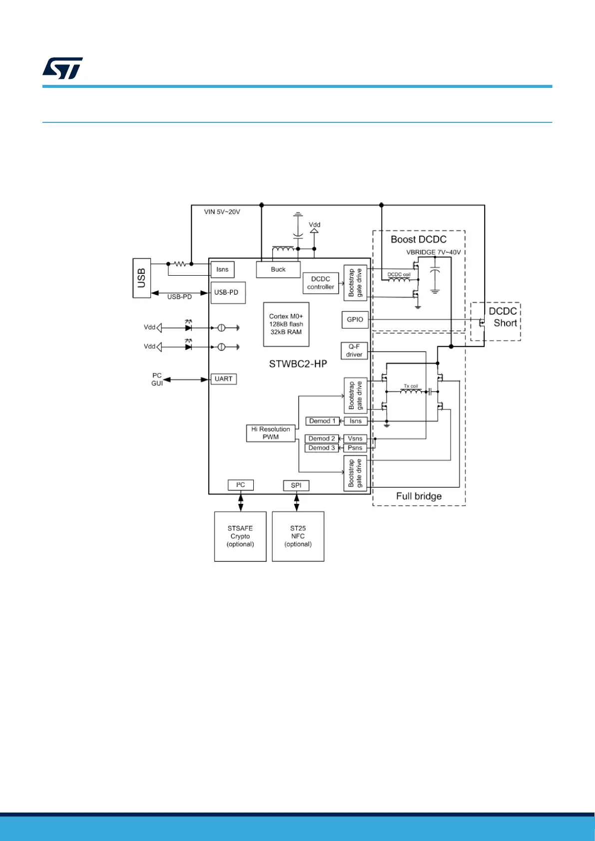
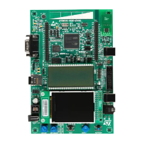
Figure 4. Block diagram
4.2 Power inverter
The power inverter is a key block in charge of converting the DC bridge voltage into an AC power signal for the
transmitting coil. The power inverter consists of four N-channel MOSFET transistors arranged into an H-bridge.
The integrated gate drivers of the STWBC2 are designed to control the inverter transistors. The gate drivers
integrate their own anti-cross-conduction circuit.
Some applications may require driving the power inverter in a half-bridge mode; for example, operating in Qi BPP
mode. STWBC2 enables switching between full-bridge and half-bridge mode operation whenever required.
4.3
ADC
STWBC2 integrates ADC to measure the preprocessed signals. The ADC is preceded by a multiplexer to access
the signals described in the following sections.
UM3286
Device description and operation
UM3286 - Rev 1
page 8/84