5.6 FW Page ....................................................................41
5.6.1 Obtaining the firmware update file ..........................................41
5.6.2 Loading the firmware into an empty device ...................................41
5.6.3 Updating firmware of a previously programmed device ...........................41
5.6.4 Calibration.............................................................41
5.6.5 Recommended flow of prototyping and production ..............................42
5.7 Protection tuning ..............................................................42
5.7.1 Foreign object detection ..................................................42
5.7.2 Static OVP ............................................................42
5.7.3 Dynamic OVP ..........................................................43
5.7.4 Current Drop OVP.......................................................43
5.7.5 Ring node overvoltage ...................................................43
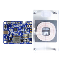
6 STEVAL-WBC2TX70 description ..................................................44
6.1 Schematic diagrams ...........................................................44
6.2 Bill of materials (BOM) .........................................................49
6.3 Component assembly..........................................................54
6.4 STEVAL-WBC2TX70 PCB layout ................................................55
6.5 STWBC2 default configuration ..................................................57
6.6 Typical performance characteristics ..............................................58
6.6.1 Power-up waveforms ....................................................58
6.6.2 Analog and digital ping ...................................................59
6.6.3 Startup of EPP .........................................................60
6.6.4 Efficiency and spatial freedom in the XY plane .................................60
6.6.5 Efficiency and spatial freedom in the Z-axis ...................................62
6.6.6 Thermal performance ....................................................63
7 Designing a wireless power transmitter based on STEVAL-WBC2TX70
evaluation board..................................................................64
7.1 BOM reduction suggestions.....................................................64
7.2 Layout guidelines .............................................................64
7.2.1 High power tracks .......................................................64
7.2.2 Ground plane on Layer 4 .................................................65
7.2.3 Board input layout .......................................................66
7.2.4 VIN, Vbuck, and Vdoubler.................................................67
7.2.5 VIN ISNS routing........................................................69
7.2.6 DC-DC boost circuit .....................................................70
7.2.7 Main bridge circuit.......................................................70
7.2.8 Bridge ISNS routing .....................................................71
UM3286
Contents
UM3286 - Rev 1
page 79/84