List of figures
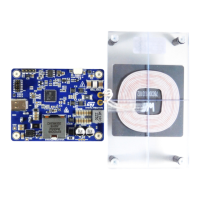
Figure 1. STEVAL-WBC2TX70 evaluation board ...................................................1
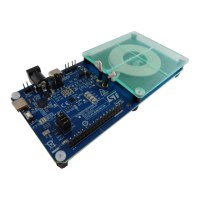
Figure 2. Board overview....................................................................4
Figure 3. Test points .......................................................................6
Figure 4. Block diagram ....................................................................8
Figure 5. Difference between BPP and EPP power transfer startup...................................... 12
Figure 6. ASK modulation ..................................................................15
Figure 7. ASK timing......................................................................15
Figure 8. Example of bit encoding.............................................................15
Figure 9. Example of byte encoding ........................................................... 16
Figure 10. Format of the three defined messages................................................... 17
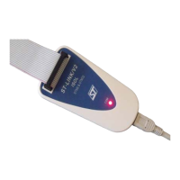
Figure 11. STLINK parameters ...............................................................19
Figure 12. Programming the chip .............................................................. 19
Figure 13. Bootloader start .................................................................. 20
Figure 14. The certificate chain process ......................................................... 24
Figure 15. The authentication process .......................................................... 24
Figure 16. The initial state of the GUI ........................................................... 27
Figure 17. Port selection ....................................................................28
Figure 18. Status semaphore................................................................. 28
Figure 19. Event box ...................................................................... 29
Figure 20. Device metrics ...................................................................33
Figure 21. Input power supply indication .........................................................33
Figure 22. Device information ................................................................35
Figure 23. Rx identification data ...............................................................35
Figure 24. Example of captured charts .......................................................... 36
Figure 25. Save and load buttons.............................................................. 37
Figure 26. Read and Write operation buttons ......................................................40
Figure 27. Save button, choosing of saved data type and Save dialog.....................................40
Figure 28. Test points ......................................................................42
Figure 29. STEVAL-WBC2TX70 circuit schematic (1 of 6) ............................................. 44
Figure 30. STEVAL-WBC2TX70 circuit schematic (2 of 6) ............................................. 45
Figure 31. STEVAL-WBC2TX70 circuit schematic (3 of 6) ............................................. 46
Figure 32. STEVAL-WBC2TX70 circuit schematic (4 of 6) ............................................. 47
Figure 33. STEVAL-WBC2TX70 circuit schematic (5 of 6) ............................................. 47
Figure 34. STEVAL-WBC2TX70 circuit schematic (6 of 6) ............................................. 48
Figure 35. Component assembly .............................................................. 54
Figure 36. PCB top layer....................................................................55
Figure 37. PCB inner1 layer ................................................................. 55
Figure 38. PCB inner2 layer ................................................................. 56
Figure 39. PCB bottom layer ................................................................. 56
Figure 40. Device power up.................................................................. 58
Figure 41. Analog and digital ping ............................................................. 59
Figure 42. Startup of EPP ................................................................... 60
Figure 43. Setup for offset test ................................................................ 61
Figure 44. X-axis offset impact on efficiency ...................................................... 61
Figure 45. Y-axis offset impact on efficiency....................................................... 62
Figure 46. Z-axis offset impact on efficiency ......................................................62
Figure 47. Thermal performance ..............................................................63
Figure 48. Layer 1 high power tracks ...........................................................64
Figure 49. Layer 4 GND .................................................................... 65
Figure 50. Placement of input connectors, filtering, and protections ......................................66
Figure 51. Larger tracks of DC-DC buck, VIN...................................................... 67
Figure 52. Green: DC-DC buck placement. Yellow: Capacitors close to STWBC2 IC........................... 68
Figure 53. VIN ISNS routing .................................................................69
UM3286
List of figures
UM3286 - Rev 1
page 81/84