Theory of
Operation-2445A/2455A
Service
U165C (from the
DAC),
changing the charging rate of
integrating capacitor C171.
When
holdoff time requirements
are
met (determined
by
the number of ramps counted), the Display Sequencer sets
the
THO
(trigger holdoff) signal
LO.
This enables both the
A Sweep hybrid (U700)
and
the A Trigger circuitry
in
U500.
The Trigger circuit begins monitoring the selected trigger
source
line
and, when a triggering event
is
detected that
meets the triggering requirements defined
by
the stored
control data, initiates the A Sweep
and
sets the TSA
(trigger status, A Sweep)
line
to Display Sequencer U650
LO
(indicating that the A Sweep has
been
triggered).
As the A Sweep circuit (U700) responds to the trigger,
it sets the
SGA
(sweep gate
A)
line
LO
(via U980A) indi-
cating that
an
A Sweep
is
in
progress. After the sweep
has
run
to completion, U700 sets the
SGA
line
HI
signaling
the
end
of sweep. The Display Sequencer then sets the
THO
line
HI,
resetting
A/8
Trigger hybrid U500
and
A
Sweep hybrid U700
in
preparation for the next sweep.
Triggers
The
A/8
Trigger hybrid (U500)
and
associated circuitry
select the triggering signal source for
each
horizontal
sweep as directed
by
the Display Sequencer.
When
the
proper triggering criteria to initiate a sweep
are
detected, a
triggering gate signal
is
produced to start the selected
sweep.
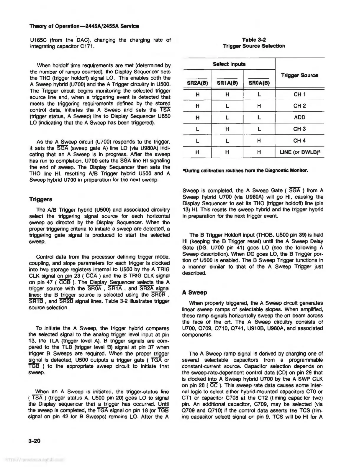
Control data from the processor defining trigger mode,
coupling,
and
slope parameters for
each
trigger
is
clocked
into two storage registers internal to U500
by
the A TRIG
CLK signal
on
pin 23 (
CCA
) and the B TRIG
CLK
signal
on
pin
47
( CCB
).
The Display Sequencer selects the A
trigger source with the SR0A , SR1A ,
and
SR2A signal
lines; the B trigger source
is
selected using the SR0B ,
SR1
B ,
and
SR2B signal lines. Table 3-2 illustrates trigger
source selection.
To initiate the A Sweep, the trigger hybrid compares
the selected signal to the analog trigger
level
input at pin
13, the TLA (trigger
level
A).
B trigger signals
are
com-
pared to the TLB (trigger
level
B)
signal at pin
37
when
trigger B Sweeps
are
required.
When
the
proper trigger
signal is
is detected, U500 outputs a trigger gate ( TGA or
TGB ) to the appropriate sweep circuit to initiate that
sweep.
When
an
A Sweep is initiated, the trigger-status line
( TSA ) (trigger status
A,
U500
pin
20)
goes
LO
to signal
the Display sequencer that a trigger
has
occurred. Until
the sweep
is
completed, the T
GA
signal
on
pin
18 (or TGB
signal
on
pin
42
for B Sweeps) remains
LO.
After the A
3-20
SR2A(B)
H
H
H
L
L
H
Table 3-2
Trigger Source Selection
Select Inputs
Trigger Source
SR1A(B) SR0A(B)
H L
CH
1
L
H
CH
2
L
L
ADD
H
L
CH
3
L
H
CH
4
H
H LINE (or BWLB)
8
•During
calibration
routines
from
the
Diagnostic
Monitor.
Sweep
is
completed, the A Sweep Gate (
SGA
) from A
Sweep hybrid U700 (via U980A) will go HI, causing the
Display Sequencer to set its
THO
(trigger holdoff)
line
(pin
13)
HI.
This resets the sweep hybrid
and
the trigger hybrid
in
preparation for the next trigger event.
The
B Trigger Holdoff input (THOB, U500 pin
39)
is
held
HI
(keeping the B Trigger reset) until the A Sweep
Delay
Gate
(DG,
U700
pin
41)
goes
LO
(see
the following A
Sweep description).
When
DG
goes
LO,
the B Trigger por-
tion of U500 is enabled. The B Sweep Trigger functions
in
a manner similar to that
of
the A Sweep Trigger just
described.
A Sweep
When
properly triggered, the A Sweep circuit generates
linear sweep ramps of selectable slopes.
When
amplified,
these ramp signals horizontally sweep the crt
beam
across
the face of the crt. The A Sweep circuitry consists of
U700, 0709, 0710, 0741, U910B, U980A,
and
associated
components.
The A Sweep ramp signal
is
derived
by
charging
one
of
several selectable capacitors from a programmable
constant-current source. Capacitor selection depends
on
the sweep-rate-dependent control data
(CD)
on
pin
29
that
is
clocked into A Sweep hybrid U700
by
the A SWP CLK
on
pin
28
(
?'.Z
).
This sweep-rate data causes some inter-
nal
logic to select either hybrid-mounted capacitors
CT0
or
CT1
or capacitor C708 at the CT2 (timing capacitor two)
pin.
An
additional capacitor, C709, may
be
selected (via
0709
and
0710) if the control data asserts the TCS (tim-
ing
capacitor select) signal
on
pin
9.
TCS will
be
HI
for A