Sweep speeds slower than 1 ms per division. Capacitor
C707
and
associated circuitry form a linearity compensa-
tion circuit.
The
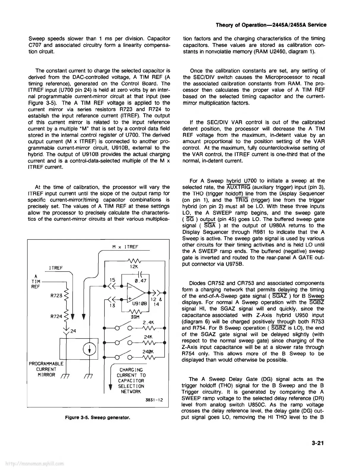
constant current to charge the selected capacitor is
derived from the DAG-controlled voltage, A TIM
REF
(A
timing reference), generated
on
the Control Board. The
ITREF input (U700
pin
24)
is
held
at zero volts
by
an
inter-
nal
programmable current-mirror circuit at that input
(see
Figure
3-5).
The
A TIM
REF
voltage is applied to the
current mirror
via
series resistors
R723
and
R724 to
establish the input reference current
(ITREF).
The
output
of this current mirror is related to the input reference
current
by
a multiple "M" that
is
set
by
a control data field
stored
in
the internal control register of U700.
The
derived
output current
(M
x
ITREF)
is
connected to another pro-
grammable current-mirror circuit,
U91
OB,
external to the
hybrid. The output of
U91
OB
provides the actual charging
current
and
is a control-data-selected multiple of the M x
ITREF current.
At the time of calibration, the processor will vary the
ITREF input current until the slope of the output ramp for
specific current-mirror/timing capacitor combinations
is
precisely set.
The
values of A TIM
REF
at these settings
allow the processor to precisely calculate the characteris-
tics of the current-mirror circuits at their various multiplica-
ITREF
A
REF
R723
R724
PROGRAMMABLE
CURRENT
MIRROR
x
ITREF
12K
39M
CHARGING
CURRENT
TO
CAPACITOR
SELECTION
NETWORK
Figure 3-5. Sweep generator.
12 &
14
3831-12
Theory
of
Operation-2445A/2455A Service
tion factors
and
the charging characteristics of the timing
capacitors. These values are stored
as
calibration con-
stants
in
nonvolatile memory (RAM U2460, diagram 1)
).
Once
the calibration constants are
set,
any setting of
the SEC/DIV switch causes the Microprocessor to recall
the associated calibration constants from
RAM.
The
pro-
cessor then calculates the proper value
of
A TIM
REF
based
on
the selected timing capacitor
and
the current-
mirror multiplication factors.
If the SEC/DIV
VAR
control
is
out of the calibrated
detent position, the processor will decrease the A TIM
REF
voltage from the maximum, in-detent
value
by
an
amount proportional to the position setting of the
VAR
control. At the maximum, fully counterclockwise setting of
the
VAR
control, the ITREF current
is
one-third that of the
normal, in-detent current.
For A Sweep hybrid U700 to initiate a sweep at the
selected rate, the AUXTRIG (auxiliary trigger) input (pin
3),
the
THO
(trigger holdoff) line from the Display Sequencer
(on
pin
1),
and
the TRIG (trigger)
line
from the trigger
hybrid
(on
pin
2)
must
all
be
LO.
With these three inputs
LO,
the A
SWEEP
ramp begins,
and
the sweep gate
(
SG
) output
(pin
45)
goes
LO.
The buffered sweep gate
signal (
SGA
)
at
the output of U980A returns to the
Display Sequencer through
R981
to indicate that the A
Sweep
is
active.
The
sweep gate signal
is
used
by
various
other circuits for their timing activities
and
is
held
LO
until
the A
SWEEP
ramp
ends. The buffered (negative) sweep
gate
is
inverted
and
routed to the rear-panel A
GATE
out-
put connector via U975B.
Diodes CR752
and
CR753
and
associated components
form a charging network that permits delaying the timing
of the end-of-A-Sweep gate signal ( SGAZ ) for B Sweep
displays. For normal A Sweep operation with the SGBZ
signal
HI,
the SGAZ signal will
end
quickly, since the
capacitance associated with 2-Axis hybrid U950 input
(diagram
6)
will
be
charged positively through both R753
and
R754.
For B Sweep operation ( SGBZ is
LO),
the
end
of the SGAZ gate signal will be delayed slightly (with
respect to the normal sweep gate) since charging of the
2-Axis input capacitance will
be
at a slower rate through
R754 only. This allows more of the B Sweep to
be
displayed than would otherwise
be
possible.
The
A Sweep
Delay
Gate
(DG)
signal acts as the
trigger holdoff
(THO)
signal for the B Sweep
and
the B
Trigger circuitry. It
is
generated
by
comparing the A
SWEEP
ramp voltage to the selected delay reference
(DR)
level
from analog switch U850C. As the ramp voltage
crosses the delay reference
level,
the delay gate
(DG)
out-
put signal goes
LO,
removing the
HI
THO
level
to the B
3-21