t
-
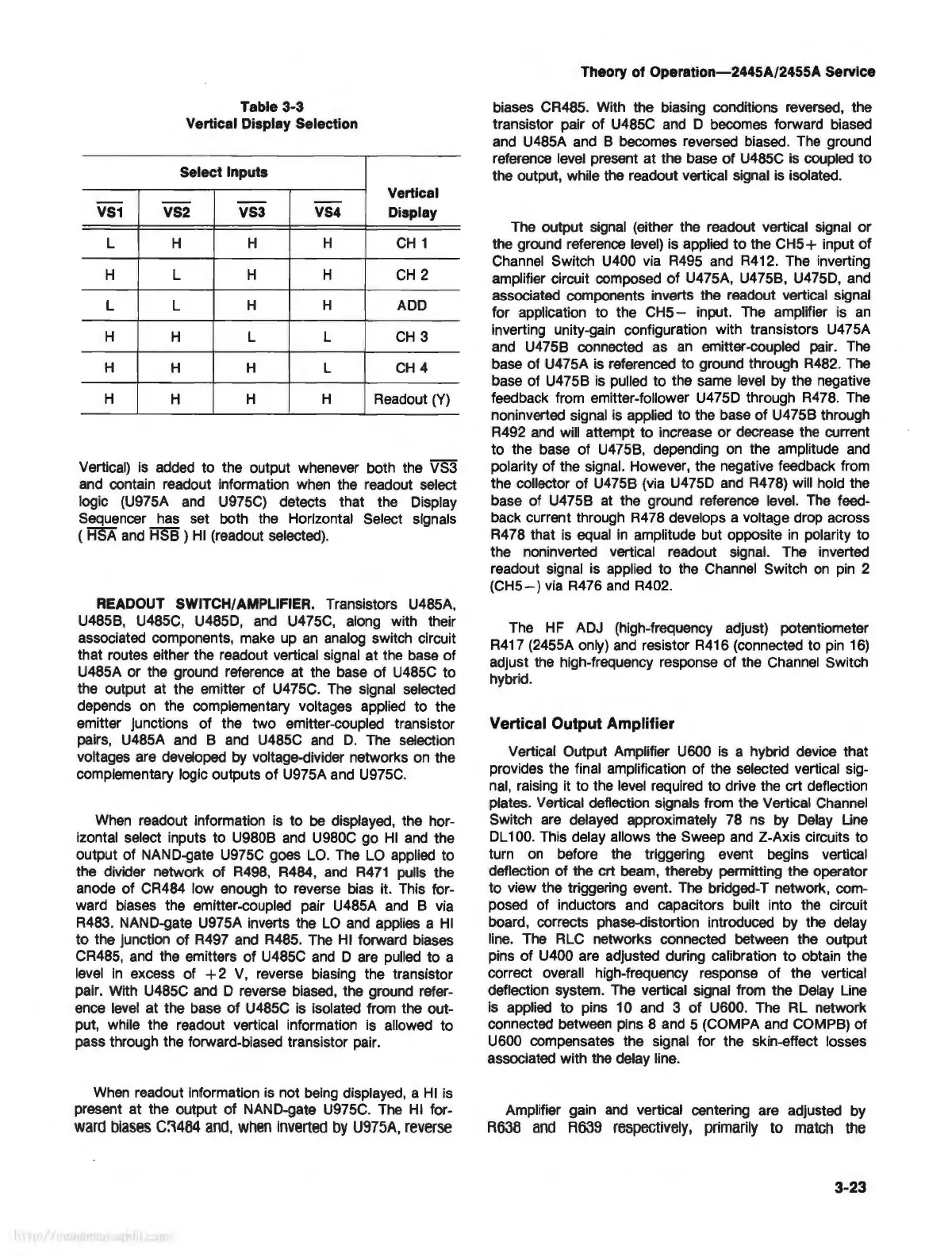
VS1
L
H
L
H
H
H
Table 3-3
Vertical Display Selection
Select Inputs
-- --
--
VS2 VS3
VS4
H
H H
L
H H
L
H H
H
L L
H
H L
H
H H
Vertical
Display
CH
1
CH
2
ADD
CH
3
CH
4
Readout
(Y)
Vertical)
is
added to the output whenever both the VS3
and
contain readout information when the readout select
logic (U97SA
and
U97SC)
detects that the Display
Sequencer has set both the Horizontal Select signals
( HSA
and
HSB )
HI
(readout selected).
READOUT SWITCH/ AMPLIFIER. Transistors U48SA,
U48SB,
U48SC,
U48SD,
and
U47SC,
along with their
associated components, make up
an
analog switch circuit
that routes either the readout vertical signal at the base of
U48SA or the ground reference at the base of
U48SC
to
the output at the emitter of
U47SC.
The signal selected
depends on the complementary voltages applied to the
emitter junctions of the two emitter-coupled transistor
pairs, U48SA
and
B
and
U48SC
and
D.
The selection
voltages are developed
by
voltage-divider networks on the
complementary logic outputs
of
U97SA and
U97SC.
When
readout information
is
to
be
displayed, the hor-
izontal select inputs to U980B
and
U980C go
HI
and
the
output of NAND-gate
U97SC
goes
LO.
The
LO
applied to
the divider network of R498, R484,
and
R471
pulls the
anode of CR484 low enough to reverse bias it. This for-
ward biases the emitter-coupled pair U48SA
and
B
via
R483. NAND-gate U97SA inverts the
LO
and
applies a
HI
to the junction of R497
and
R48S.
The
HI
forward biases
CR48S,
and
the emitters of
U48SC
and
D are pulled to a
level
in
excess of
+2
V,
reverse biasing the transistor
pair. With
U48SC
and
D reverse biased, the ground refer-
ence
level
at the base of
U48SC
is
isolated from the out-
put, while the readout vertical information
is
allowed to
pass through the forward-biased transistor pair.
When
readout information is not being displayed, a
HI
is
present at the output of NAND-gate
U97SC.
The
HI
for-
ward
biases
CR484
and,
when
inverted
by
U975A,
reverse
II
Theory of
Operation-2445A/2455A
Service
biases CR48S. With the biasing conditions reversed, the
transistor pair of
U48SC
and
D becomes forward biased
and
U48SA
and
B becomes reversed biased. The ground
reference level present at the base of
U48SC
is
coupled
to
the output, while the readout vertical signal
is
isolated.
The output signal (either the readout vertical signal or
the ground reference level) is applied
to
the CHS+ input of
Channel Switch U400
via
R49S
and
R412. The inverting
amplifier circuit composed of U47SA, U47SB,
U47SD,
and
associated components inverts the readout vertical signal
for application to the
CHS
- input. The amplifier
is
an
inverting unity-gain configuration with transistors U47SA
and
U47SB
connected as
an
emitter-coupled pair. The
base of U47SA is referenced to ground through R482. The
base of U47SB
is
pulled to the same
level
by
the negative
feedback from emitter-follower
U47SD
through R478. The
noninverted signal
is
applied to the base of U47SB through
R492
and
will attempt to increase or decrease the current
to the base of
U47SB,
depending
on
the amplitude
and
polarity of the signal. However, the negative feedback from
the collector of
U47SB
(via
U47SD
and
R478) will hold the
base of U47SB
at
the ground reference level. The feed-
back current through R478 develops a voltage drop across
R478 that
is
equal
in
amplitude but opposite
in
polarity to
the noninverted vertical readout signal. The inverted
readout signal is applied to the Channel Switch
on
pin
2
(CHS-)
via
R476
and
R402.
The
HF
ADJ (high-frequency adjust) potentiometer
R417
(24SSA
only)
and
resistor R416 (connected to
pin
16)
adjust the high-frequency response of the Channel Switch
hybrid.
Vertical Output Amplifier
Vertical Output Amplifier U600
is
a hybrid device that
provides the final amplification of the selected vertical sig-
nal, raising it to the level required to drive the crt deflection
plates. Vertical deflection signals from the Vertical Channel
Switch are delayed approximately 78 ns
by
Delay
Line
DL
100. This delay allows the Sweep
and
Z-Axis circuits to
turn
on
before the triggering event begins vertical
deflection of the crt beam, thereby permitting the operator
to view the triggering event.
The
bridged-T network, com-
posed of inductors
and
capacitors built into the circuit
board, corrects phase-distortion introduced
by
the delay
line. The
RLC
networks connected between the output
pins of U400 are adjusted during calibration
to
obtain the
correct overall high-frequency response of the vertical
deflection system. The vertical signal from the
Delay
Line
is
applied to pins 10
and
3 of U600. The RL network
connected between pins 8
and
s (COMPA
and
COMPS) of
U600 compensates the signal for the skin-effect losses
associated with the delay line.
Amplifier gain
and
vertical centering are adjusted
by
R638
and
R639
respectively,
primarily
to
match
the
3-23