Theory
of
Operation-2445A/2455A
Service
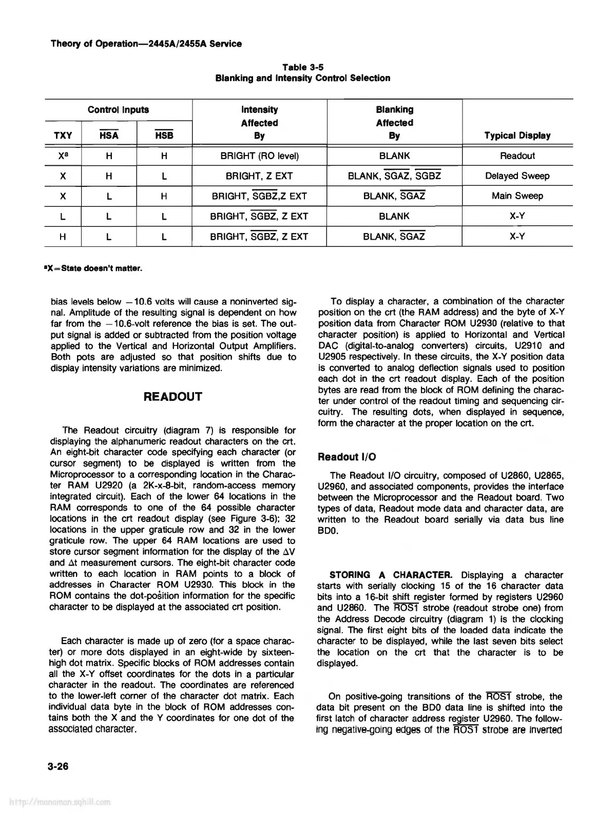
Table 3-5
Blanking and Intensity Control Selection
Control Inputs
Intensity
Affected
--
--
TXY
HSA
HSB
By
xa
H H BRIGHT
(RO
level)
X H
L
BRIGHT, Z
EXT
--
X
L
H BRIGHT, SGBZ,Z
EXT
--
L
L
L
BRIGHT, SGBZ, Z
EXT
--
H
L L
BRIGHT, SGBZ, Z
EXT
•X=State
doesn't matter.
bias
levels below
-10.6
volts will cause a noninverted sig-
nal.
Amplitude of the resulting signal
is
dependent
on
how
far from the
-10.6-volt
reference the
bias
is set. The out-
put signal
is
added
or subtracted from the position voltage
applied to the Vertical
and
Horizontal Output Amplifiers.
Both pots are adjusted so that position shifts due to
display intensity variations
are
minimized.
READOUT
The
Readout circuitry (diagram
7)
is responsible for
displaying the alphanumeric readout characters
on
the crt.
An
eight-bit character code specifying each character (or
cursor segment) to
be
displayed
is
written from the
Microprocessor to a corresponding location
in
the Charac-
ter
RAM
U2920
(a
2K-x-8-bit, random-access memory
integrated circuit).
Each
of the lower
64
locations
in
the
RAM
corresponds to one of the
64
possible character
locations
in
the crt readout display
(see
Figure 3-6);
32
locations
in
the upper graticule row
and
32
in
the lower
graticule row.
The
upper
64
RAM
locations are used to
store cursor segment information for the display of the
þÿ”V
V
and
þÿ”t
measurement cursors. The eight-bit character code
written to
each
location
in
RAM
points to a block of
addresses
in
Character
ROM
U2930. This block
in
the
ROM
contains the dot-position information for the specific
character to
be
displayed at the associated crt position.
Each
character
is
made
up
of zero (for a space charac-
ter) or more dots displayed
in
an
eight-wide
by
sixteen-
high dot matrix. Specific blocks of
ROM
addresses contain
all
the
X-Y
offset coordinates for the dots
in
a particular
character
in
the readout.
The
coordinates are referenced
to the lower-left corner of the character dot matrix.
Each
individual data byte
in
the block of
ROM
addresses con-
tains both the X
and
the Y coordinates for one dot of the
associated
character.
3-26
Blanking
Affected
By
Typical Display
BLANK
Readout
----
BLANK, SGAZ, SGBZ
Delayed
Sweep
BLANK, SGAZ
Main Sweep
BLANK
X-Y
--
BLANK,SGAZ
X-Y
To display a character, a combination of the character
position
on
the crt (the RAM address)
and
the byte of
X-Y
position data from Character
ROM
U2930 (relative to that
character position)
is
applied to Horizontal and Vertical
DAC
(digital-to-analog converters) circuits, U2910
and
U2905 respectively.
In
these circuits, the
X-Y
position data
is
converted to analog deflection signals used to position
each
dot
in
the crt readout display.
Each
of the position
bytes
are
read
from the block of
ROM
defining the charac-
ter under control of the readout timing
and
sequencing cir -
cuitry.
The
resulting dots, when displayed
in
sequence,
form the character at the proper location
on
the crt.
Readout 1/0
The Readout 1/0 circuitry, composed of U2860, U2865,
U2960,
and
associated components, provides the interface
between the Microprocessor
and
the Readout board. Two
types of data, Readout mode data
and
character data,
are
written to the Readout board serially via data
bus
line
BD0.
STORING
A CHARACTER. Displaying a character
starts with serially clocking
15
of the
16
character data
bits into a 16-bit shift register formed by registers U2960
and
U2860.
The
ROS1
strobe (readout strobe
one)
from
the Address Decode circuitry (diagram
1)
is the clocking
signal.
The
first eight bits of the loaded data indicate the
character to
be
displayed, while the last
seven
bits select
the location
on
the crt that the character
is
to
be
displayed.
On
positive-going transitions of the
F«5sT
strobe, the
data bit present
on
the BD0 data line
is
shifted into the
first latch of character address register U2960. The follow-
ing
negative-going
edges
of
the
ROS1
strobe
are
inverted