Specifications
1- 6
CSA7404B, TDS7704B, TDS7404B, TDS7254B & TDS7154B Service Manual
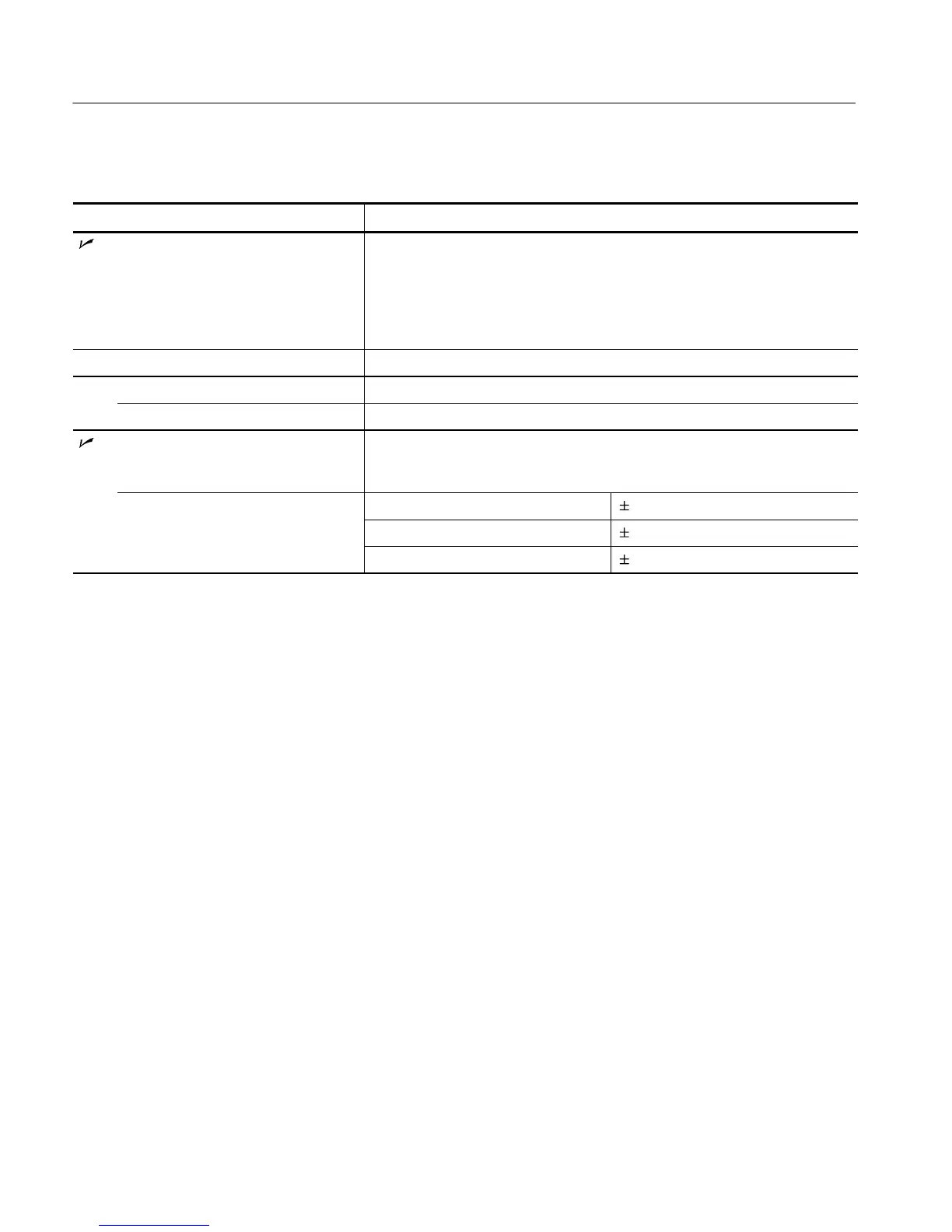
Table 1- 2: Channel input and vertical specifications ( Cont.)
noitpircseDcitsiretcarahC
Maximum input voltage, <1 V
RMS for <100 mV/division settings and
CSA7404B, TDS7404B, TDS7154B, &
TDS7254B
TDS7704B
<5 V
RMS for
≥ 100 mV settings
<6.5 V
RMS for
≥
100 mV settings for t emperatrues
≤
45 °
C
<6.0 V
RMS for
≥
100 mV settings for t emperatrues
> 45
°
C
Number of digitized bits 8 bits
Sensitivity range Fine adjustment available with
≥1% resol ution
2 mV/div to 1 V/divi sion, in a 1-2-5 sequence
DC gain accuracy Net offset is the nominal voltage that must be appl ied to the channel t o bring the
trace to center screen. Net offset = off set -- (position× volts/division) and is
expressed in volts
TDS7704B 2 mV/div to 3.98 mV/div (3% +(6%× | net offset/1V | ))
4 mV/div to 99.5 mV/div (2.5% +(2%× | net offset/1V | ))
100 mV/div to 1 V/div (2.5% +(2%× | net offset/10V | ))
 Loading...