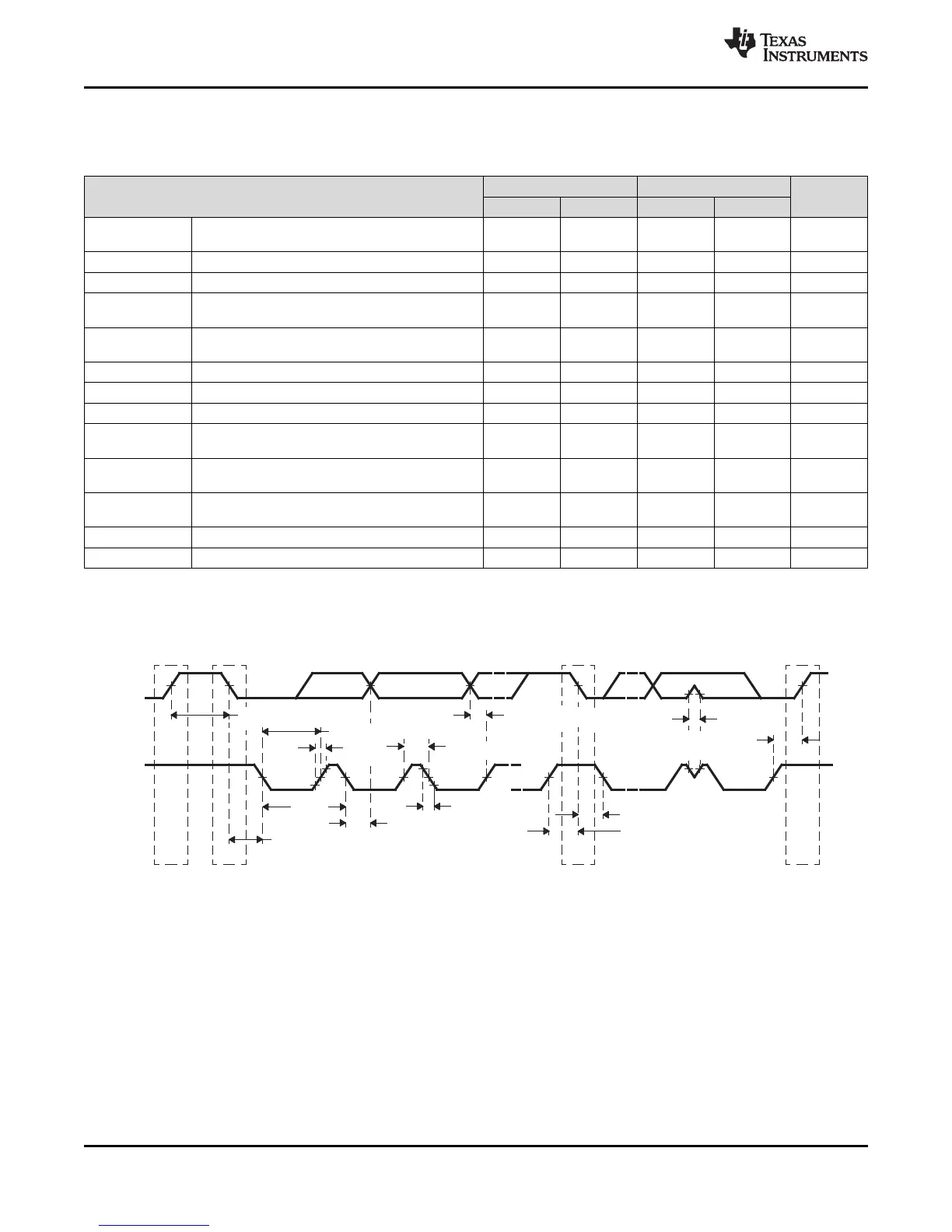
SDA
SCL
t
w(SDAH)
t
w(SCLL)
t
w(SCLH)
t
w(SP)
t
h(SCLL-SDAL)
t
h(SDA-SCLL)
t
h(SCLL-SDAL)
t
su(SCLH-SDAL)
t
f(SCL)
t
c(SCL)
t
r(SCL)
t
su(SCLH-SDAH)
Stop Start Repeated Start Stop
t
su(SDA-SCLH)
130
TMS570LS0714
SPNS226E –JUNE 2013–REVISED NOVEMBER 2016
www.ti.com
Submit Documentation Feedback
Product Folder Links: TMS570LS0714
Peripheral Information and Electrical Specifications Copyright © 2013–2016, Texas Instruments Incorporated
(1) The I2C pins SDA and SCL do not feature fail-safe I/O buffers. These pins could potentially draw current when the device is powered
down.
(2) The maximum t
h(SDA-SCLL)
for I2C-bus devices has only to be met if the device does not stretch the low period (t
w(SCLL)
) of the SCL
signal.
(3) C
b
= The total capacitance of one bus line in pF.
7.11.2 I2C I/O Timing Specifications
Table 7-31. I2C Signals (SDA and SCL) Switching Characteristics
(1)
PARAMETER
STANDARD MODE FAST MODE
UNIT
MIN MAX MIN MAX
t
c(I2CCLK)
Cycle time, internal module clock for I2C,
prescaled from VCLK
75.2 149 75.2 149 ns
f
(SCL)
SCL clock frequency 0 100 0 400 kHz
t
c(SCL)
Cycle time, SCL 10 2.5 µs
t
su(SCLH-SDAL)
Setup time, SCL high before SDA low (for a
repeated START condition)
4.7 0.6 µs
t
h(SCLL-SDAL)
Hold time, SCL low after SDA low (for a repeated
START condition)
4 0.6 µs
t
w(SCLL)
Pulse duration, SCL low 4.7 1.3 µs
t
w(SCLH)
Pulse duration, SCL high 4 0.6 µs
t
su(SDA-SCLH)
Setup time, SDA valid before SCL high 250 100 ns
t
h(SDA-SCLL)
Hold time, SDA valid after SCL low (for I2C-bus
devices)
0 3.45
(2)
0 0.9 µs
t
w(SDAH)
Pulse duration, SDA high between STOP and
START conditions
4.7 1.3 µs
t
su(SCLH-SDAH)
Setup time, SCL high before SDA high (for STOP
condition)
4.0 0.6 µs
t
w(SP)
Pulse duration, spike (must be suppressed) 0 50 ns
C
b
(3)
Capacitive load for each bus line 400 400 pF
Figure 7-19. I2C Timings
 Loading...


