43
TMS570LS0714
www.ti.com
SPNS226E –JUNE 2013–REVISED NOVEMBER 2016
Submit Documentation Feedback
Product Folder Links: TMS570LS0714
System Information and Electrical SpecificationsCopyright © 2013–2016, Texas Instruments Incorporated
6 System Information and Electrical Specifications
6.1 Device Power Domains
The device core logic is split up into multiple power domains to optimize the power for a given application
use case. There are five core power domains: PD1, PD2, PD3, PD5, and RAM_PD1. See Section 1.4 for
more information.
PD1 is an "always-ON" power domain, which cannot be turned off. Each of the other core power domains
can be turned ON/OFF one time during device initialization as per the application requirement. Refer to
the Power Management Module (PMM) chapter of the device technical reference manual for more details.
NOTE
The clocks to a module must be turned off before powering down the core domain that
contains the module.
6.2 Voltage Monitor Characteristics
A voltage monitor is implemented on this device. The purpose of this voltage monitor is to eliminate the
requirement for a specific sequence when powering up the core and I/O voltage supplies.
6.2.1 Important Considerations
• The voltage monitor does not eliminate the need of a voltage supervisor circuit to ensure that the device is held in
reset when the voltage supplies are out of range.
• The voltage monitor only monitors the core supply (VCC) and the I/O supply (VCCIO). The other supplies are not
monitored by the VMON. For example, if the VCCAD or VCCP are supplied from a source different from that for
VCCIO, then there is no internal voltage monitor for the VCCAD and VCCP supplies.
6.2.2 Voltage Monitor Operation
The voltage monitor generates the Power Good MCU signal (PGMCU) as well as the I/Os Power Good IO
signal (PGIO) on the device. During power-up or power-down, the PGMCU and PGIO are driven low when
the core or I/O supplies are lower than the specified minimum monitoring thresholds. The PGIO and
PGMCU signals being low isolates the core logic as well as the I/O controls during power up or power
down of the supplies. This allows the core and I/O supplies to be powered up or down in any order.
When the voltage monitor detects a low voltage on the I/O supply, it will assert a power-on reset. When
the voltage monitor detects an out-of-range voltage on the core supply, it asynchronously makes all output
pins high impedance, and asserts a power-on reset. The voltage monitor is disabled when the device
enters a low power mode.
The VMON also incorporates a glitch filter for the nPORRST input. Refer to Section 6.3.3.1 for the timing
information on this glitch filter.
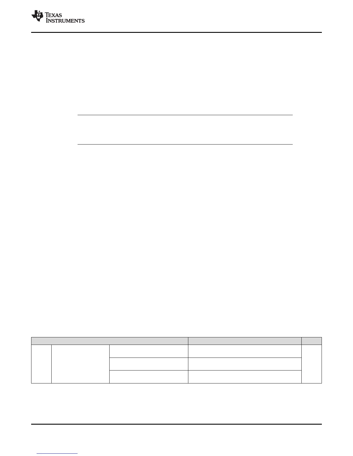
Table 6-1. Voltage Monitoring Specifications
PARAMETER MIN TYP MAX UNIT
V
MON
Voltage monitoring
thresholds
VCC low - VCC level below this
threshold is detected as too low.
0.75 0.9 1.13
V
VCC high - VCC level above this
threshold is detected as too high.
1.40 1.7 2.1
VCCIO low - VCCIO level below this
threshold is detected as too low.
1.85 2.4 2.9