t
f
t
r
V
CCIO
V
OH
V
OH
V
OL
V
OL
0
Output
94
TMS570LS0714
SPNS226E –JUNE 2013–REVISED NOVEMBER 2016
www.ti.com
Submit Documentation Feedback
Product Folder Links: TMS570LS0714
Peripheral Information and Electrical Specifications Copyright © 2013–2016, Texas Instruments Incorporated
Table 7-2. Switching Characteristics for Output Timings versus Load Capacitance (C
L
) (continued)
PARAMETER MIN MAX UNIT
Rise time, t
r
Selectable 8 mA / 2 mA-z pins
(see Table 4-40)
8mA mode
CL = 15 pF 2.5
ns
CL = 50 pF 4
CL = 100 pF 7.2
CL = 150 pF 12.5
Fall time, t
f
CL = 15 pF 2.5
CL = 50 pF 4
CL = 100 pF 7.2
CL = 150 pF 12.5
Rise time, t
r
2mA-z mode
CL = 15 pF 8
CL = 50 pF 15
CL = 100 pF 23
CL = 150 pF 33
Fall time, t
f
CL = 15 pF 8
CL = 50 pF 15
CL = 100 pF 23
CL = 150 pF 33
(1) This specification does not account for any output buffer drive strength differences or any external capacitive loading differences. Check
Table 4-40 for output buffer drive strength information on each signal.
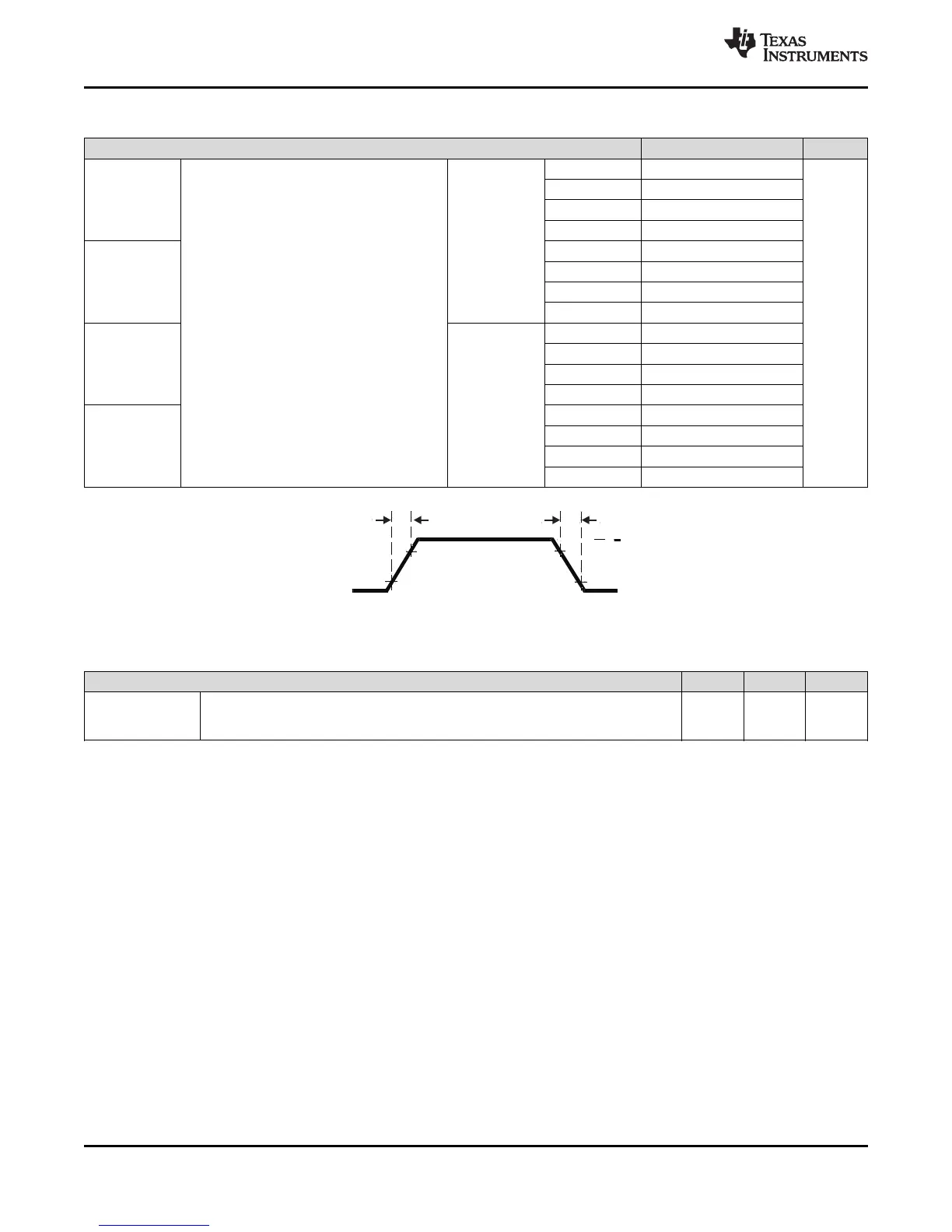
Figure 7-2. CMOS-Level Outputs
Table 7-3. Timing Requirements for Outputs
(1)
MIN MAX UNIT
t
d(parallel_out)
Delay between low-to-high, or high-to-low transition of general-purpose output
signals that can be configured by an application in parallel, for example, all signals in
a GIOA port, or all N2HET1 signals, and so forth
6 ns