151
TMS570LS0714
www.ti.com
SPNS226E –JUNE 2013–REVISED NOVEMBER 2016
Submit Documentation Feedback
Product Folder Links: TMS570LS0714
Device and Documentation SupportCopyright © 2013–2016, Texas Instruments Incorporated
9.9 Device Identification
9.9.1 Device Identification Code Register
The device identification code register at address 0xFFFFFFF0 identifies several aspects of the device
including the silicon version. The details of the device identification code register are shown in Table 9-1.
The device identification code register value for this device is:
• Rev 0 = 0x8052AD05
• Rev A = 0x8052AD0D
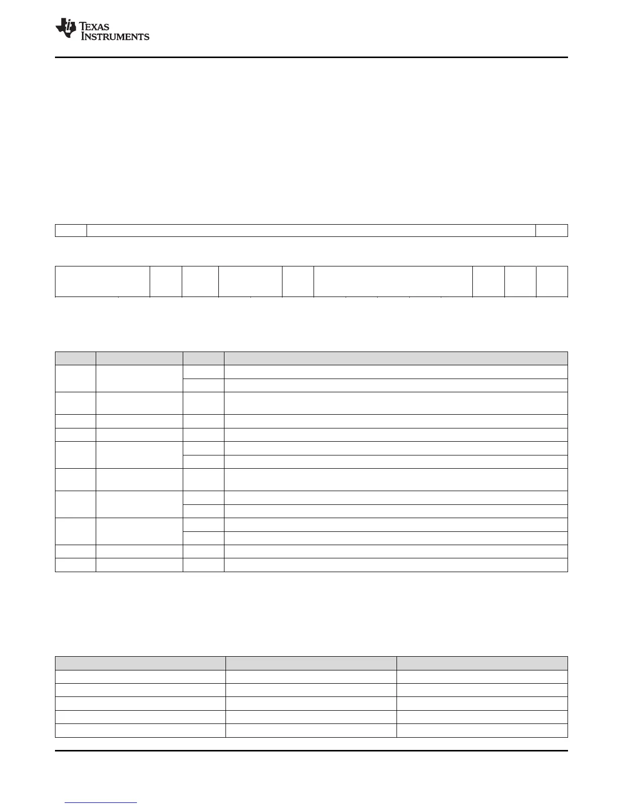
Figure 9-2. Device ID Bit Allocation Register
31 30 29 28 27 26 25 24 23 22 21 20 19 18 17 16
CP15 UNIQUE ID TECH
R-1 R-00000000101001 R-0
15 14 13 12 11 10 9 8 7 6 5 4 3 2 1 0
TECH I/O
VOLT
AGE
PERIPH
PARITY
FLASH ECC RAM
ECC
REVISION 1 0 1
R-101 R-0 R-1 R-10 R-1 R-00000 R-1 R-0 R-1
LEGEND: R/W = Read/Write; R = Read only; -n = value after reset
Table 9-1. Device ID Bit Allocation Register Field Descriptions
BIT FIELD VALUE DESCRIPTION
31 CP15
Indicates the presence of coprocessor 15
1 CP15 present
30-17 UNIQUE ID 101001
Unique device identification number
This bitfield holds a unique number for a dedicated device configuration (die).
16-13 TECH Process technology on which the device is manufactured.
0101 F021
12 I/O VOLTAGE
I/O voltage of the device.
0 I/O are 3.3 V
11 PERIPH PARITY 1
Peripheral Parity
Parity on peripheral memories
10-9 FLASH ECC
Flash ECC
10 Program memory with ECC
8 RAM ECC
Indicates if RAM ECC is present.
1 ECC implemented
7-3 REVISION Revision of the Device.
2-0 101 The platform family ID is always 0b101
9.9.2 Die Identification Registers
The two die ID registers at addresses 0xFFFFFF7C and 0xFFFFFF80 form a 64-bit dieid with the
information as shown in Table 9-2.
Table 9-2. Die-ID Registers
ITEM NO. OF BITS BIT LOCATION
X Coord. on Wafer 12 0xFFFFFF7C[11:0]
Y Coord. on Wafer 12 0xFFFFFF7C[23:12]
Wafer # 8 0xFFFFFF7C[31:24]
Lot # 24 0xFFFFFF80[23:0]
Reserved 8 0xFFFFFF80[31:24]
 Loading...


