7 Series FPGAs GTP Transceivers User Guide www.xilinx.com 179
UG482 (v1.9) December 19, 2016
RX Buffer Bypass
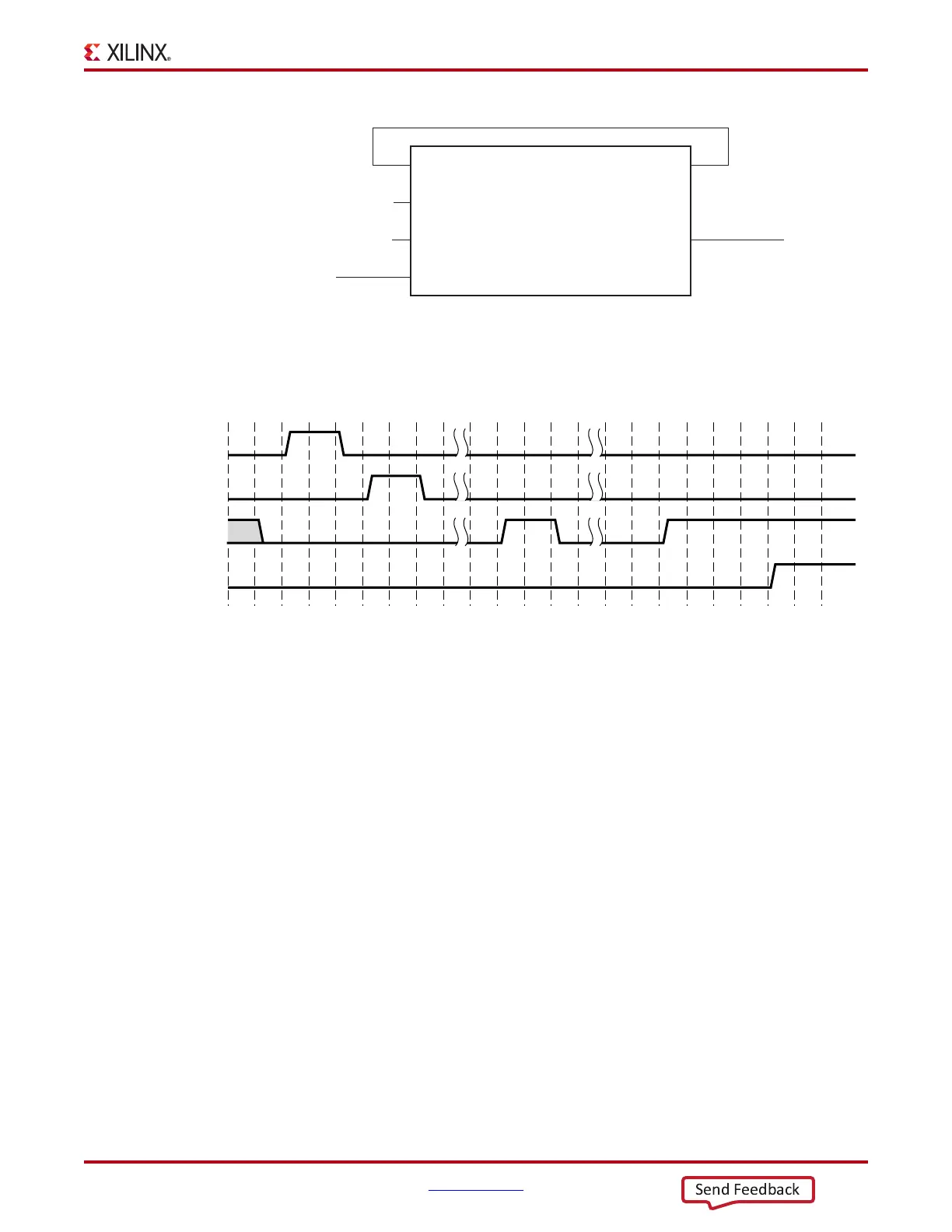
Figure 4-37 shows the required steps to perform the auto RX phase alignment and use the RX delay
alignment to adjust RXUSRCLK to compensate for temperature and voltage variations.
Notes relevant to Figure 4-37:
1. The sequence of events in Figure 4-37 is not drawn to scale.
2. After conditions such as a GTP receiver reset or RX rate change, RX phase alignment must be
performed to align XCLK and RXUSRCLK. Wait until exiting RXELECIDLE and RX CDR is
locked before asserting RXDLYSRESET to start the RX phase and delay alignments. The
assertion of RXDLYSRESET should be less than 50 ns.
3. Wait until RXDLYSRESETDONE is High. RXDLYSRESETDONE will stay asserted for a
minimum of 100 ns.
4. When RXSYNCDONE is asserted, the alignment procedure is completed. This signal will
remain asserted until the alignment procedure is re-initiated.
5. Upon the assertion of RXSYNCDONE, RXPHALIGNDONE indicates whether alignment is
achieved and maintained.
6. RX delay alignment continues to adjust RXUSRCLK to compensate for temperature and
voltage variations.
It is necessary to start the RX phase alignment after RX CDR is locked to ensure that the RX
recovered clock and RXUSRCLK are stable and ready to be used for alignment. When the RX
elastic buffer is bypassed, data received from the PMA can be distorted due to phase differences
after conditions such as a GTP transceiver reset or rate change. If the received data evaluated at the
fabric interface is invalid, the RX phase alignment needs to be repeated while the RX CDR is
locked.
X-Ref Target - Figure 4-36
Figure 4-36: RX Buffer Bypass—Single-Lane, Auto Mode Port Connection
RXSYNCMODE
RXSYNCALLIN
RXSYNCIN RXSYNCOUT
UG482_c4_136_020613
RXSYNCDONE
RXPHALIGNDONE
1'b1
1'b0
RXDLYSRESET
X-Ref Target - Figure 4-37
Figure 4-37: RX Buffer Bypass Example—Single-Lane Auto Mode
RXDLYSRESET
RXDLYSRESETDONE
RXPHALIGNDONE
RXSYNCDONE
UG482_c4_137_020613

 Loading...


