180 www.xilinx.com 7 Series FPGAs GTP Transceivers User Guide
UG482 (v1.9) December 19, 2016
Chapter 4: Receiver
Using RX Buffer Bypass in Multi-Lane Manual Mode
For GTP transceivers, phase alignment can be performed manually or automatically.
This section describes the steps required to perform the multi-lane RX buffer bypass alignment
procedure manually:
• Master: In a multi-lane application, the buffer bypass master is the lane that is the source of
RXOUTCLK.
• Slave: All the lanes that share the same RXUSRCLK/RXUSRCLK2, which is generated from
the RXOUTCLK of the buffer bypass master.
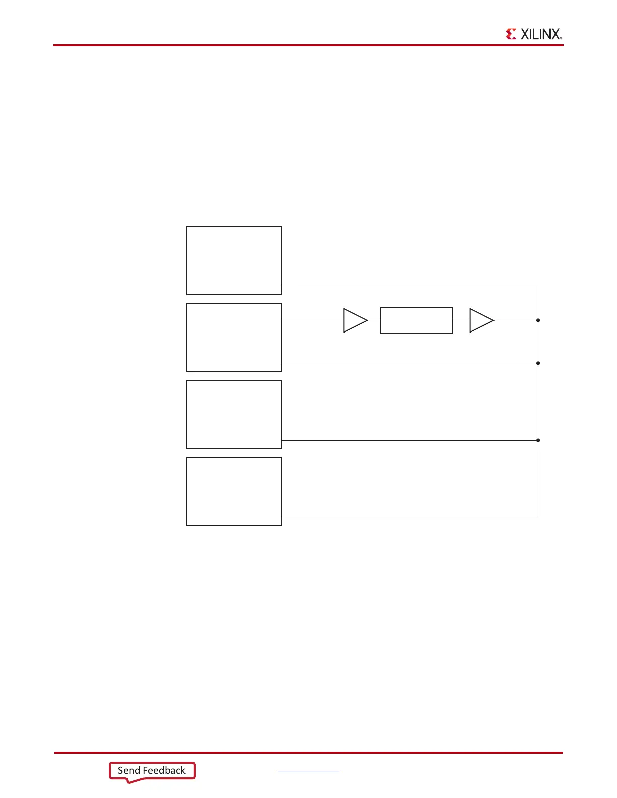
Figure 4-38 shows an example of buffer bypass master versus slave lanes.
These GTP transceiver settings should be used to bypass the RX elastic buffer:
• RXBUF_EN = FALSE
• RX_XCLK_SEL = RXUSR
• RXOUTCLKSEL = 010 to select the RX recovered clock as the source of RXOUTCLK
• RXDDIEN = 1
With the RX recovered clock selected, RXOUTCLK is to be used as the source of RXUSRCLK.
The user must ensure that RXOUTCLK and the selected RX recovered clock are operating at the
desired frequency. When the RX elastic buffer is bypassed, the RX phase alignment procedure must
be performed after these conditions:
• Resetting or powering up the GTP transceiver receiver
X-Ref Target - Figure 4-38
Figure 4-38: Example of RX Buffer Bypass Master versus Slave Lanes
UG482_c4_138_020613
BUFG BUFG
GTP RX
Lane 3
Slave
RXUSRCLK
RXUSRCLK2
GTP RX
Lane 2
MMCM/PLL
Master
RXUSRCLK
RXOUTCLK
RXUSRCLK2
GTP RX
Lane 1
Slave
RXUSRCLK
RXUSRCLK2
GTP RX
Lane 0
Slave
RXUSRCLK
RXUSRCLK2