7 Series FPGAs GTP Transceivers User Guide www.xilinx.com 181
UG482 (v1.9) December 19, 2016
RX Buffer Bypass
• Resetting or powering up the PLL
• Changing the RX recovered clock source or frequency
• Changing the GTP transceiver RX line rate
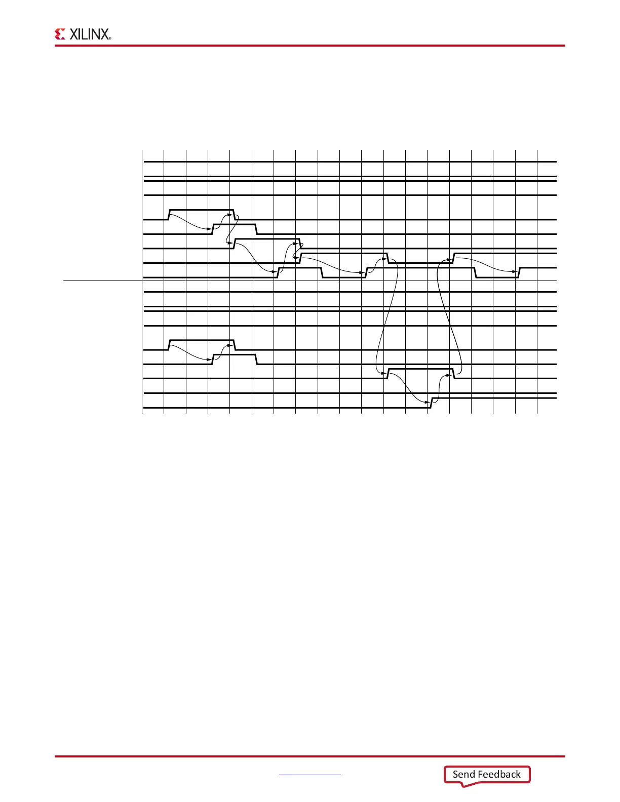
Figure 4-39 shows the required steps to perform manual RX phase and delay alignment.
Notes relevant to Figure 4-39:
1. The sequence of events shown in Figure 4-39 is not drawn to scale.
2. M_* denotes ports related to the master lane.
3. S_* denotes ports related to the slave lane(s).
4. Set the RXSYNC_OVRD attribute to 1'b1.
5. Set RXPHDLYRESET and RXDLYBYPASS to Low for all lanes.
6. Set RXPHALIGNEN and RXDDIEN to High for all lanes.
7. Assert RXDLYSRESET for all lanes. Hold this signal High until RXDLYSRESETDONE of
the respective lane is asserted.
8. Deassert RXDLYSRESET for the lane in which the RXDLYSRESETDONE is asserted.
9. When RXDLYSRESET of all lanes are deasserted, assert RXPHALIGN for the master lane.
Hold this signal High until the rising edge of RXPHALIGNDONE of the master lane is
observed.
10. Deassert RXPHALIGN for the master lane.
11. Assert RXDLYEN for the master lane. This causes RXPHALIGNDONE to be deasserted.
12. Hold RXDLYEN for the master lane High until the rising edge of RXPHALIGNDONE of the
master lane is observed.
X-Ref Target - Figure 4-39
Figure 4-39: RX Phase and Delay Alignment in Manual Mode
M_RXPHDLYRESET
M_RXDLYBYPASS
M_RXPHALIGNEN
M_RXDDIEN
M_RXDLYSRESET
M_RXDLYSRESETDONE
M_RXPHALIGN
M_RXDLYEN
M_RXPHALIGNDONE
S_RXPHDLYRESET
S_RXDLYBYPASS
S_RXPHALIGNEN
S_RXDDIEN
S_RXDLYSRESET
S_RXDLYSRESETDONE
S_RXPHALIGN
S_RXDLYEN
S_RXPHALIGNDONE
UG482_c4_39_020713