26 www.xilinx.com 7 Series FPGAs GTP Transceivers User Guide
UG482 (v1.9) December 19, 2016
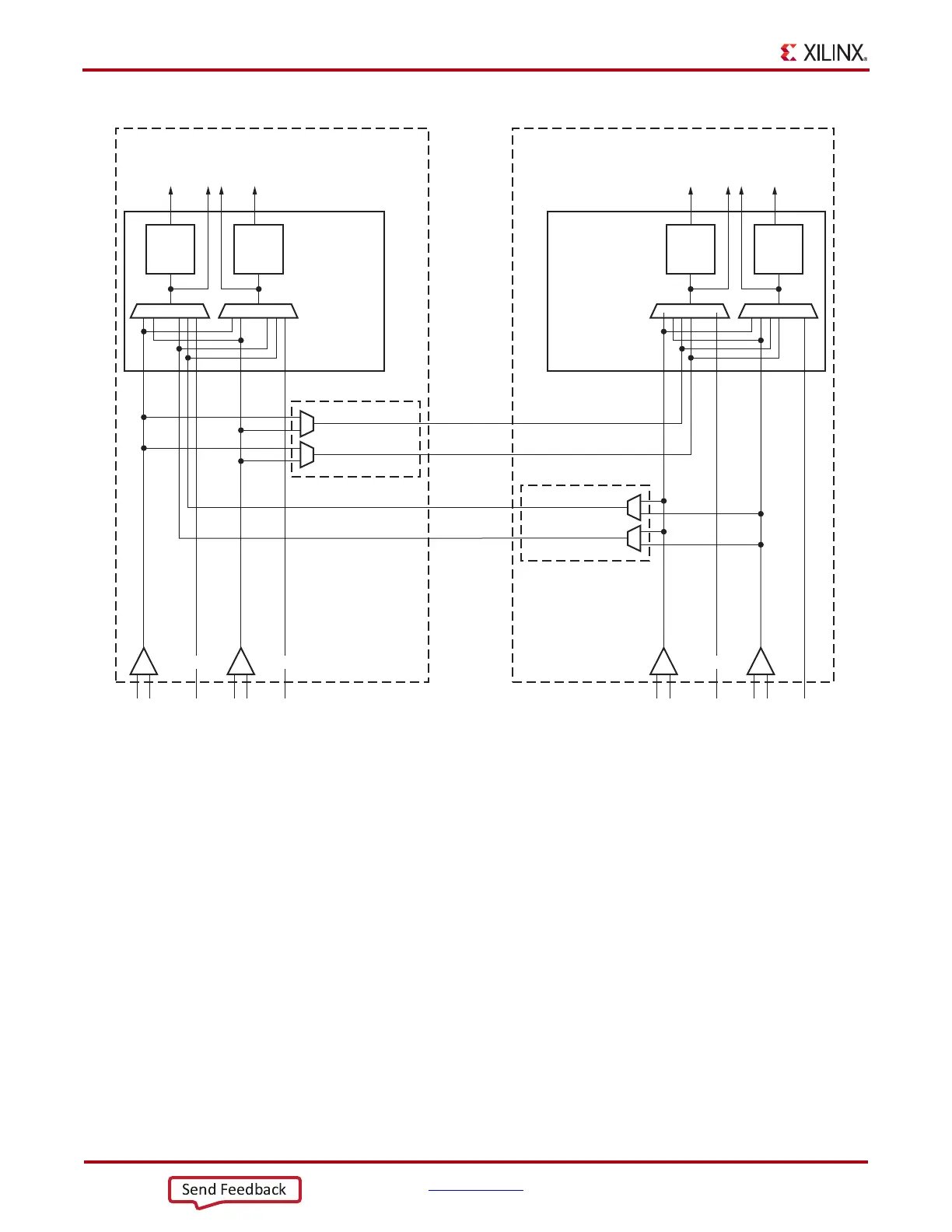
Chapter 2: Shared Features
Figure 2-3 shows the shows the detailed view of the reference clock multiplexer structures within a
single GTPE2_COMMON primitive. The PLL0REFCLKSEL and PLL1REFCLKSEL ports are
required when multiple reference clock sources are connected to the multiplexers. A single
reference clock is most commonly used. In this case, the PLL[0/1]REFCLKSEL port can be tied to
3'b001, and the Xilinx software tools handle the complexity of the multiplexers and associated
routing. See External Reference Clock Use Model, page 31 for more information.
X-Ref Target - Figure 2-2
Figure 2-2: Conceptual View of GTP Transceiver Reference Clocking
UG482_c2_01_012413
PLL0
To GTPE2_CHANNEL
GTPE2_
COMMON_
X0Y0
PLL1
1234567 1234567
GTEASTREFCLK0
Controlled by Software
GTEASTREFCLK1
GTP Quad
PLL0
To GTPE2_CHANNEL
GTPE2_
COMMON_
X1Y0
PLL1
1234567 1234567
GTWESTREFCLK1
Controlled by Software
GTWESTREFCLK0
GTP Quad
MGTREFCLK0P
MGTREFCLK0N
IBUFDS_GTE2
GTGREFCLK0
GTGREFCLK1
GTREFCLK0
GTREFCLK1
GTGREFCLK0
GTGREFCLK1
GTREFCLK0
GTREFCLK1
MGTREFCLK1P
MGTREFCLK1N
MGTREFCLK0P
MGTREFCLK0N
MGTREFCLK1P
MGTREFCLK1N
IBUFDS_GTE2IBUFDS_GTE2 IBUFDS_GTE2