7 Series FPGAs GTP Transceivers User Guide www.xilinx.com 27
UG482 (v1.9) December 19, 2016
Reference Clock Selection and Distribution
Ports and Attributes
Table 2-4 and Table 2-5 define the clocking ports and attributes for the GTPE2_COMMON
primitive.
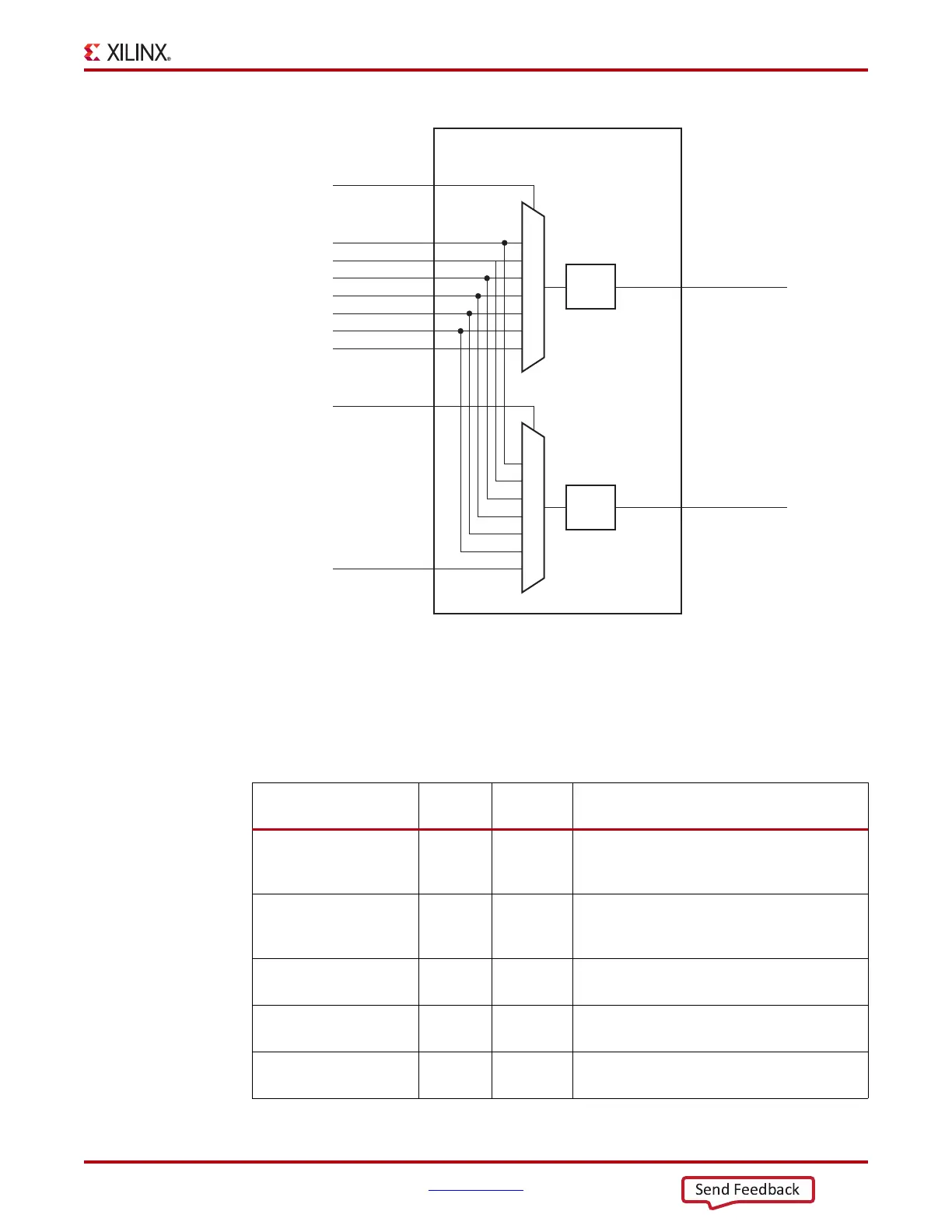
X-Ref Target - Figure 2-3
Figure 2-3: PLL0 and PLL1 Reference Clock Selection Multiplexer
UG482_c2_03_112811
PLL0
PLL0 Output CLK
0
GTPE2_COMMON
GTREFCLK0
1
GTREFCLK1
PLL1
PLL1 Output CLK
2
GTEASTREFCLK0
3
4
GTEASTREFCLK1
5
GTWESTREFCLK0
6
GTWESTREFCLK1
7
GTGREFCLK0
GTGREFCLK1
PLL1REFCLKSEL[2:0]
PLL0REFCLKSEL[2:0]
0
1
2
3
4
5
6
7
Table 2-4: GTPE2_COMMON Clocking Ports
Port Direction
Clock
Domain
Description
GTGREFCLK0 In Clock Reference clock generated by the internal
FPGA logic. This input is reserved for internal
testing purposes only.
GTGREFCLK1 In Clock Reference clock generated by the internal
FPGA logic. This input is reserved for internal
testing purposes only.
GTREFCLK0 In Clock External clock driven by IBUFDS_GTE2 for
PLL0 and/or PLL1.
GTREFCLK1 In Clock External clock driven by IBUFDS_GTE2 for
PLL0 and/or PLL1.
GTWESTREFCLK0 In Clock West-bound clock from the Quad on the right
side of the device.