28 www.xilinx.com 7 Series FPGAs GTP Transceivers User Guide
UG482 (v1.9) December 19, 2016
Chapter 2: Shared Features
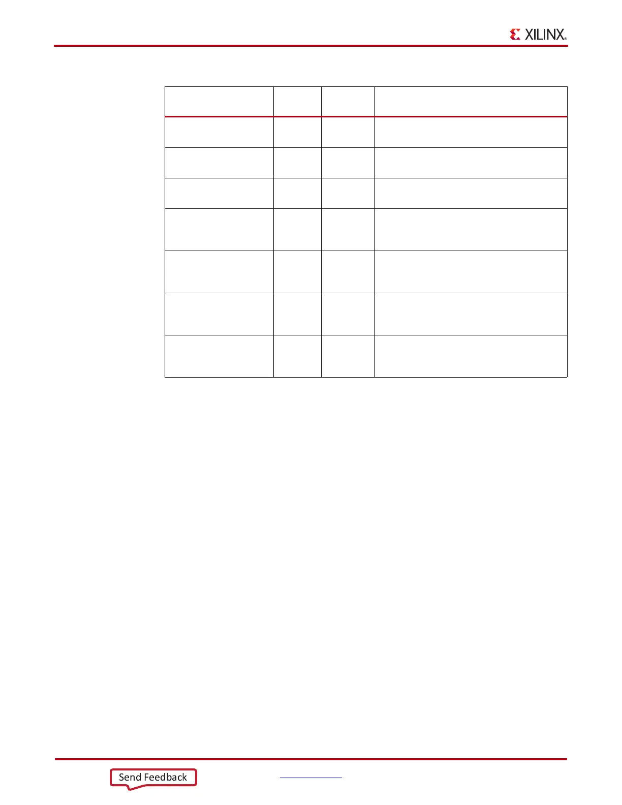
GTWESTREFCLK1 In Clock West-bound clock from the Quad on the right
side of the device.
GTEASTREFCLK0 In Clock East-bound clock from the Quad on the left side
of the device.
GTEASTREFCLK1 In Clock East-bound clock from the Quad on the left side
of the device.
PLL0OUTCLK Out Clock PLL0 clock output. The user must connect this
port to the PLL0CLK port on the
GTPE2_CHANNEL primitive.
PLL1OUTCLK Out Clock PLL1 clock output. The user must connect this
port to the PLL1CLK port on the
GTPE2_CHANNEL primitive.
PLL0OUTREFCLK Out Clock The user must connect this port to the
PLL0REFCLK port on the GTPE2_CHANNEL
primitive.
PLL1OUTREFCLK Out Clock The user must connect this port to the
PLL1REFCLK port on the GTPE2_CHANNEL
primitive.
Table 2-4: GTPE2_COMMON Clocking Ports (Cont’d)
Port Direction
Clock
Domain
Description