54 www.xilinx.com 7 Series FPGAs GTP Transceivers User Guide
UG482 (v1.9) December 19, 2016
Chapter 2: Shared Features
4. Issue a DRP write to the GTPE2_CHANNEL primitive, DRPADDR 9‘h011, set bit[11] to
1’b0.
a. To ensure only bit[11] of DRPADDR 9‘h011 is modified, it is best to perform a
read-modify-write function.
5. Upon DRP write completion, the user can set and hold GTRXRESET Low as desired. The user
can extend the assertion of GTRXRESET, as long as GTRXRESET is held High until the DRP
write is completed.
Note:
It is recommended to use the associated PLLLOCK from either the PLL0 or PLL1 to
release GTRXRESET from High to Low as shown in Figure 2-19.
6. Wait for the falling edge of RXPMARESETDONE.
7. Issue a DRP write to the GTPE2_CHANNEL primitive, DRPADDR 9‘h011, restoring the
original setting for bit[11]. The completion of this DRP write must occur before
RXPMARESETDONE switches from Low to High. RXPMARESETDONE stays Low for a
minimum of 0.66 µs.
8. GTRXRESET should be driven with an output of a register to avoid glitches.
9. RXPMARESET_TIME should be set to 5’h3. This should be the default setting.
10. The sequence above will simulate correctly if SIM_RESET_SPEEDUP is set to FALSE. If
SIM_RESET_SPEEDUP is set to TRUE, the above sequence should be bypassed.
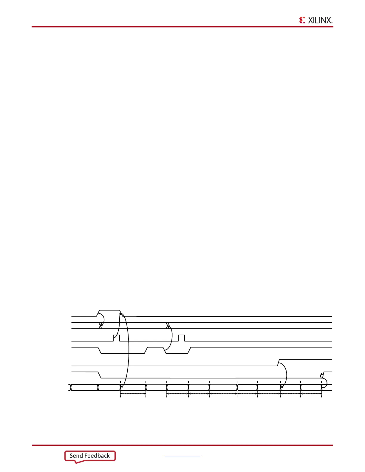
GTP Transceiver RX Reset in Response to GTRXRESET Pulse
The GTP transceiver allows the user to completely reset the entire GTP transceiver’s RX at any time
when needed by sending GTRXRESET an active High pulse. All RX reset attributes listed in
Table 2-18 can be set statically or reprogrammed through DRP ports to adjust the required reset time
before applying GTRXRESET. These conditions must be met to use GTRXRESET:
1. GTRESETSEL must be driven Low to use sequential mode.
2. All reset inputs shown on the left of
Figure 2-18 including RXPMARESET, RXCDRRESET,
RXCDRFREQRESET, RXLPMRESET, EYESCANRESET, RXPCSRESET, and
RXBUFRESET must be constantly driven Low during the entire reset process before
RXRESETDONE is detected High.
3. The associated PLL must indicate locked.
4. The steps for issuing GTRXRESET is illustrated in
Figure 2-20.
X-Ref Target - Figure 2-20
Figure 2-20: GTP Transceiver Receiver Reset after GTRXRESET Pulse
UG482_c2_120_021113
IDLE RXPMARESET RXCDRFREQRESET IDLE
GTRXRESET
RXRESETDONE
WAIT RXCDRRESET RXLPMRESET RXISCANRESET RXPCSRESET RXBUFRESET
RXPMARESETDONE
DRPRDY
RXOSCALWAIT
restore setting
1’b0
DRP
wr (addr ‘h011, bit[11])
RXOSCALRESET
_TIME
RXMPARRESET
_TIME
RXCDRPHRESET
_TIME
RXCDRFREQRESET
_TIME
RXUSERRDY
RX RESET FSM
RXLPMRESET
_TIME
RXISCANRESET
_TIME
RXMPARRESET
_TIME
RXPCSRESET
_TIME
RXBUFRESET
_TIME