68 www.xilinx.com 7 Series FPGAs GTP Transceivers User Guide
UG482 (v1.9) December 19, 2016
Chapter 2: Shared Features
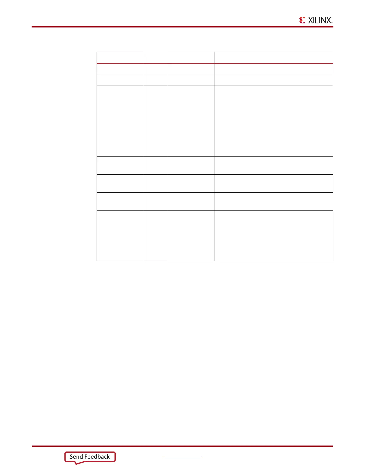
Table 2-30: DRP Ports of GTPE2_COMMON
Port Dir Clock Domain Description
DRPADDR[7:0] In DRPCLK DRP address bus.
DRPCLK In N/A DRP interface clock.
DRPEN In DRPCLK DRP enable signal.
0: No read or write operation performed.
1: Enables a read or write operation.
For write operations, DRPWE and DRPEN must
be driven High for one DRPCLK cycle only (see
Figure 2-23 for correct operation). For read
operations, DRPEN must be driven High for one
DRPCLK cycle only (see Figure 2-24 for correct
operation).
DRPDI[15:0] In DRPCLK Data bus for writing configuration data from the
FPGA logic resources to the transceiver.
DRPRDY Out DRPCLK Indicates operation is complete for write
operations and data is valid for read operations.
DRPDO[15:0] Out DRPCLK Data bus for reading configuration data from the
GTP transceiver to the FPGA logic resources.
DRPWE In DRPCLK DRP write enable.
0: Read operation when DRPEN is 1.
1: Write operation when DRPEN is 1.
For write operations, DRPWE and DRPEN must
be driven High for one DRPCLK cycle only.
Please see Figure 2-23 for correct operation.