7 Series FPGAs GTP Transceivers User Guide www.xilinx.com 69
UG482 (v1.9) December 19, 2016
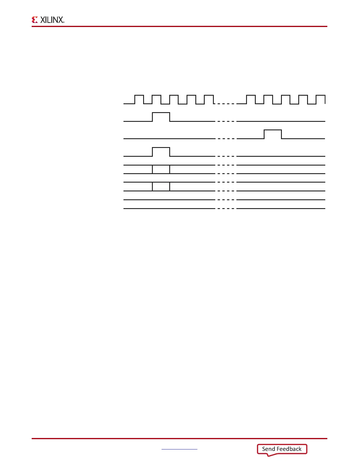
Dynamic Reconfiguration Port
Usage Model
Write Operation
Figure 2-23 shows the DRP write operation timing. New DRP operation can be initiated when
DRPRDY is asserted.
Read Operation
Figure 2-24 shows the DRP read operation timing. New DRP operation can be initiated when
DRPRDY is asserted.
X-Ref Target - Figure 2-23
Figure 2-23: DRP Write Timing
UG482_c2_12_040213
(1)
(1) After a DRP write is requested, it takes 5 DRPCLK clock cycles
for the DRPRDY signal to be asserted.
DRPCLK
DRPEN
DRPRDY
DRPWE
DRPADDR
DRPDI
DRPDO
ADR
DAT

 Loading...


