7 Series FPGAs GTP Transceivers User Guide www.xilinx.com 81
UG482 (v1.9) December 19, 2016
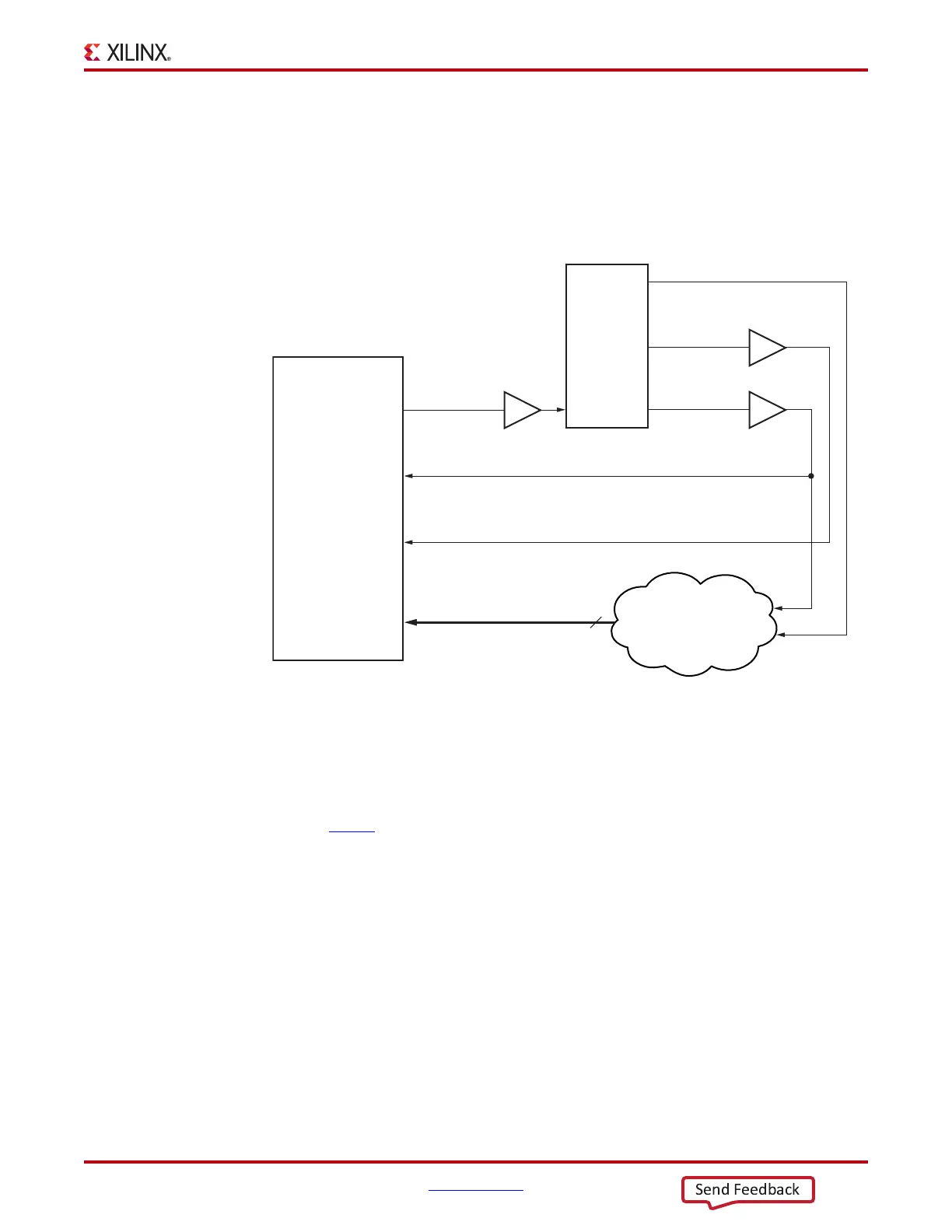
FPGA TX Interface
TXOUTCLK Driving GTP Transceiver TX in 4-Byte Mode
In Figure 3-4, TXOUTCLK is used to drive TXUSRCLK2 for 4-byte mode (TX_DATA_WIDTH =
32 or 40). The frequency of TXUSRCLK2 is equal to half of the frequency of TXUSRCLK.
MMCMs or PLLs, which are part of the clock management tiles (CMTs) located in the top half of
the device, can only drive the BUFGs in the top half of the devices. Similarly, MMCMs or PLLs
located in the bottom half can only drive BUFGs in the bottom half.
Notes relevant to Figure 3-4:
1. F
TXUSRCLK2
= F
TXUSRCLK
/2
2. In the XC7A200T device, BUFH can be used with certain limitations. For details about
placement constraints and restrictions on clocking resources (MMCM, BUFH, BUFG, etc.),
refer to UG472
, 7 Series FPGAs Clocking Resources User Guide.
X-Ref Target - Figure 3-4
Figure 3-4: Single Lane—TXOUTCLK Drives TXUSRCLK2 (4-Byte Mode)
UG482_c3_04_041012
BUFG
or BUFH
1
7 Series FPGAs
GTP Transceiver
TXOUTCLK
TXUSRCLK2
CLKIN
1
TXUSRCLK
TXDATA (32 / 40 bits)
Design in
FPGA
MMCME2
or
PLLE2
BUFG
2
CLKOUT0
BUFG
2
CLKOUT1
LOCKED