82 www.xilinx.com 7 Series FPGAs GTP Transceivers User Guide
UG482 (v1.9) December 19, 2016
Chapter 3: Transmitter
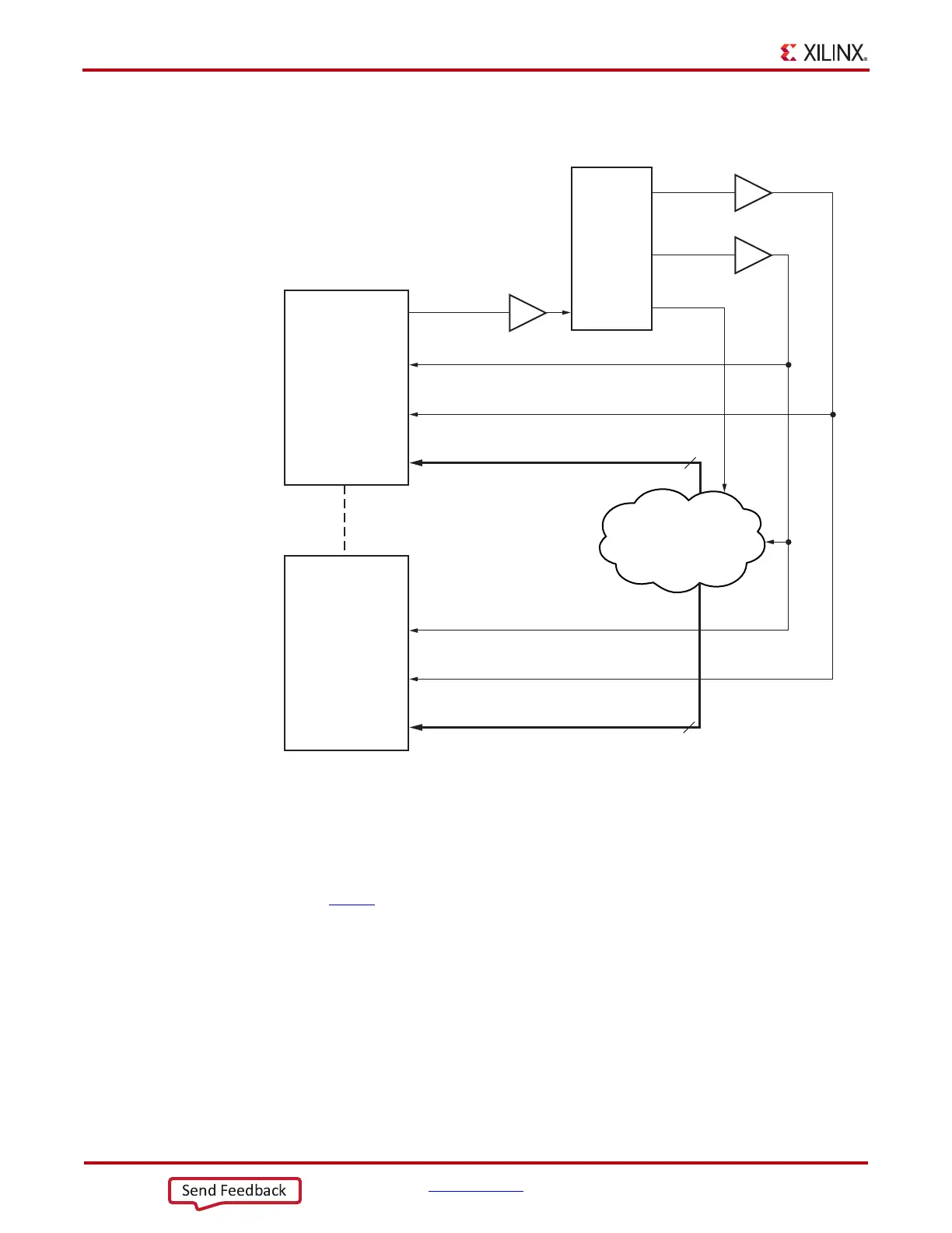
Similarly, Figure 3-5 shows the shows the same settings in multiple lanes configuration.
Notes relevant to Figure 3-5:
1. F
TXUSRCLK2
= F
TXUSRCLK
/2.
2. In the XC7A200T device, BUFH can be used with certain limitations. For details about
placement constraints and restrictions on clocking resources (MMCM, BUFH, BUFG, etc.),
refer to UG472
, 7 Series FPGAs Clocking Resources User Guide.
X-Ref Target - Figure 3-5
Figure 3-5: Multiple Lanes—TXOUTCLK Drives TXUSRCLK2 (4-Byte Mode)
UG482_c3_05_041012
BUFG
or BUFH
1
Artix-7 FPGA
GTP Transceiver
TXOUTCLK
TXUSRCLK2
CLKIN
1
TXUSRCLK
TXDATA (TX_DATA_WIDTH = 32 / 40 bits)
Design in
FPGA
TXDATA (TX_DATA_WIDTH = 32 / 40 bits)
MMCME2
or
PLLE2
1
Artix-7 FPGA
GTP Transceiver
TXUSRCLK2
1
TXUSRCLK
BUFG
2
CLKOUT0
BUFG
2
CLKOUT1
LOCKED