88 www.xilinx.com 7 Series FPGAs GTP Transceivers User Guide
UG482 (v1.9) December 19, 2016
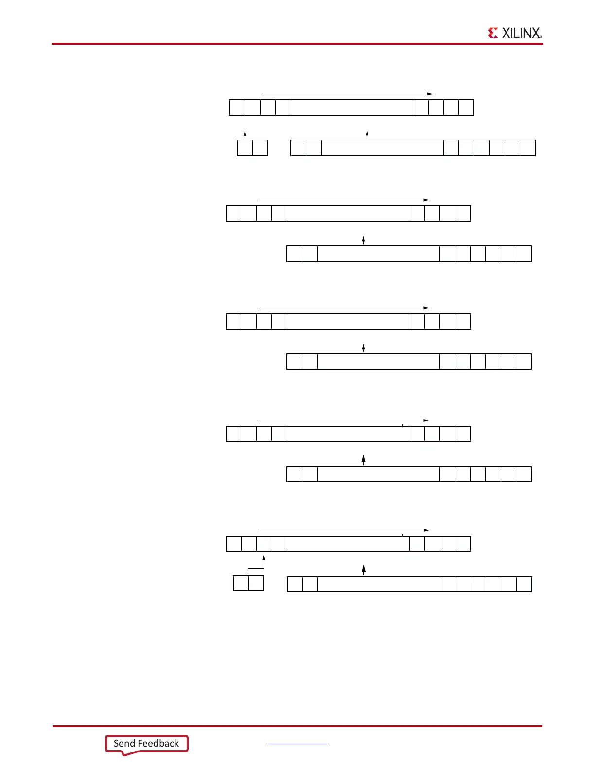
Chapter 3: Transmitter
Note relevant to Figure 3-7:
1. Per IEEE802.3ae nomenclature, H1 corresponds to TxB<0>, H0 to TxB<1>, etc.
X-Ref Target - Figure 3-7
Figure 3-7: TX Gearbox Bit Ordering
UG482_c3_07_110911
H1 H0
D15 D14 D5 D4 D3 D2
………………………
Transmitted
First
Transmitted
Last
Transmitted
First
Transmitted
Last
Transmitted
First
Transmitted
Last
Transmitted
First
Transmitted
Last
H1 H0
D15 D14 D5 D4 D3 D2……………………… D1 D0
TXDATATXHEADER
Output of the TXGearbox
Cycle 0
D1 D0
D15 D14 D5 D4 D3 D2………………………
D15 D14 D5 D4 D3 D2
………………………
D1 D0
TXDATA
Output of the TXGearbox
Cycle 1
D1 D0
D15 D14 D5 D4 D3 D2
………………………
H1 H0
D15 D14 D5 D4 D3 D2
………………………
D1 D0
TXDATA
TXHEADER
Output of the TXGearbox
Cycle 2
D1 D0
D15 D14 D5 D4 D3 D2
………………………
D15 D14 D5 D4 D3 D2
………………………
D1 D0
TXDATA
Output of the TXGearbox
Cycle 3
Transmitted
First
Transmitted
Last
D1 D0
H1 H0 D7 D6 D5 D4
………………………
D15 D14 D5 D4 D3 D2
………………………
D1 D0
TXDATA
Output of the TXGearbox
Cycle 4