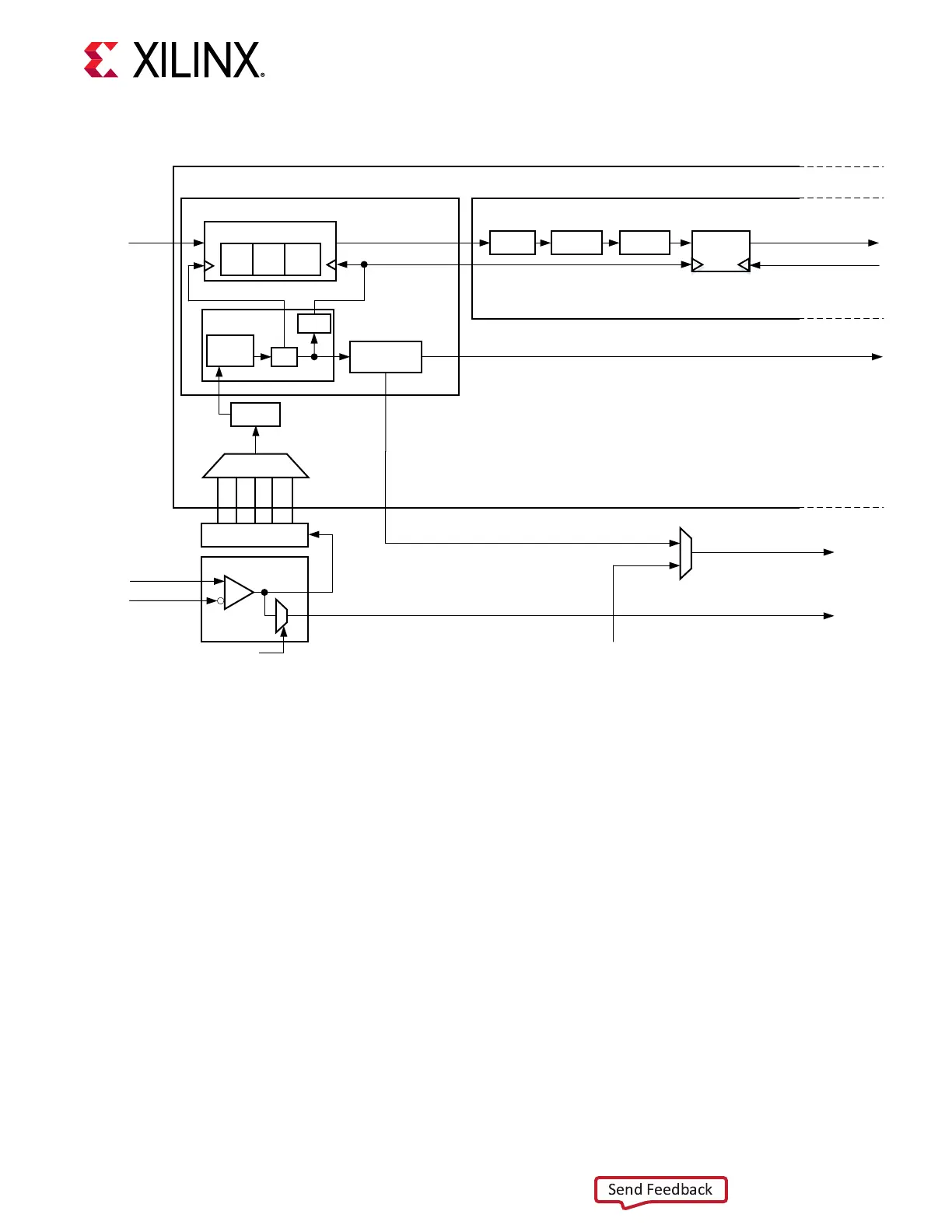
Figure 41: RX Serial and Parallel Clock Divider
IBUFDS_GTM
MGTREFCLKP
MGTREFCLKN
ODIV2
O
REFCLK_HROW_CK_SEL
REFCLK Distribution
REFCLK SEL
LCPLL
RX PROG
DIV
TXP/N
RX DATA
RX PCSRX PMA
RX DATA to Downstream
PCS Blocks
Output Clock to BUFG_GT
Output to
GTM_DUAL
GTM_DUAL (GTM Transceiver Primitive)
Phase
Interp.
RX CLKGEN
/2
SIPO
ADC DSP CDR
/16
Output to
MGTREFCLK Pad
RXRECCLK[0/1] from the other GTM RX
channel within the same GTM_DUAL
Gray
Decoder
Pre-
Coder
Polarity
Control
RXRECCLK[0/1]
RX FIFO
CH[0/1]_RXUSRCLK
CH[0/1]_RXPROGDIVCLK
X20927-110218
Notes relevant to the gure:
1. CH[0/1]_RXPROGDIVCLK is used as the source of the interconnect logic clock via BUFG_GT.
2. There is only one LCPLL in the GTM_DUAL primive which is shared between the TX/RX.
3. RXRECCLK[0/1] is the same as CH[0/1]_RXPROGDIVCLK. It can be routed to the
MGTREFCLK output pad to be used elsewhere.
RX Programmable Divider
The RX programmable divider shown in Figure 41 uses the LCPLL output clock to generate a
parallel output clock. By using the transceiver LCPLL, RX programmable divider, and BUFG_GT,
CH[0/1]_RXPROGDIVCLK should be used as a clock source for the interconnect logic.
The following tables show the programmable divider ports and aributes, respecvely.
Chapter 4: Receiver
UG581 (v1.0) January 4, 2019 www.xilinx.com
Virtex UltraScale+ GTM Transceivers 95
 Loading...

