xiC - Technical Manual Version 1.16
3.10.3. Optically isolated Digital Input
3.10.3.1. Optically isolated Digital Input - General info
Effect of incorrect input terminal connection
Reverse voltage polarity protected
Effects when withdrawing/inserting input
module under power
Maximum recommended cable length
Input level for logical 0
Voltage < 2.0V/Current 0mA to 0.3mA
Input level for logical 1
Voltage > 4.0V/Current 4mA to 6mA
Input delay – rising edge
1.7 +/-0.2µs (V
INPUT
=10V, T
AMBIENT
=25°C)
Input delay – falling edge
1
10.7 +/-0.2µs (V
INPUT
=10V, T
AMBIENT
=25°C)
Trigger, get current level (rising or falling edge are supported)
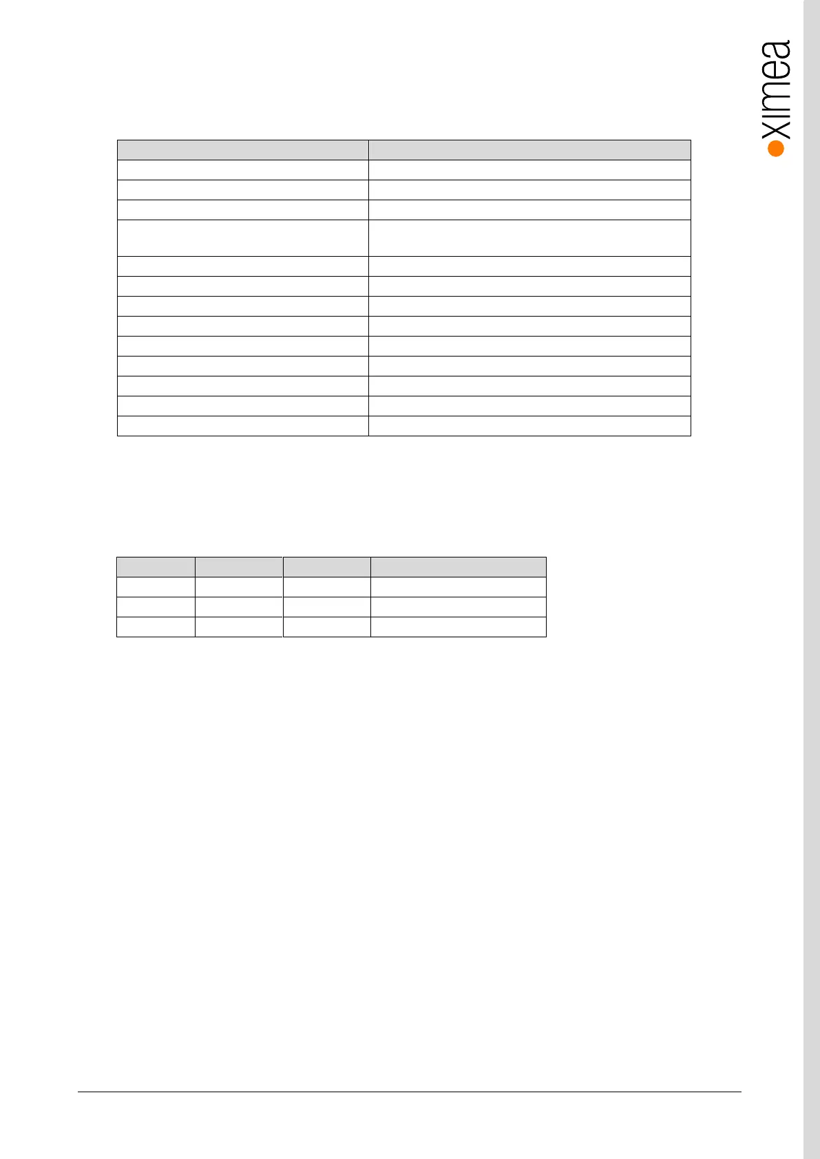
table 3-32, Optically isolated digital input, general info
Note: – 1) Propagation delay depends on voltage level, propagation jitter is significantly lower.
3.10.3.2. Digital Input – signal levels
Input levels are not IEC 61131-2, Type 1 as the ON state has been extended to support 5V TTL
0.0 – 0.3 mA (0mA nominal)
table 3-33, digital info, signal levels
Note:
• Input level Vin represents amplitude of the input signal.
• Voltage levels referenced to common ground GND