xiC - Technical Manual Version 1.16
3.10.5. Non-isolated Digital Lines (-UB and -TC only)
Non isolated Digital lines can be used as inputs or outputs compatible with TTL logic. These are high impedance pins so when
used as output high impedance slave input has to be used.
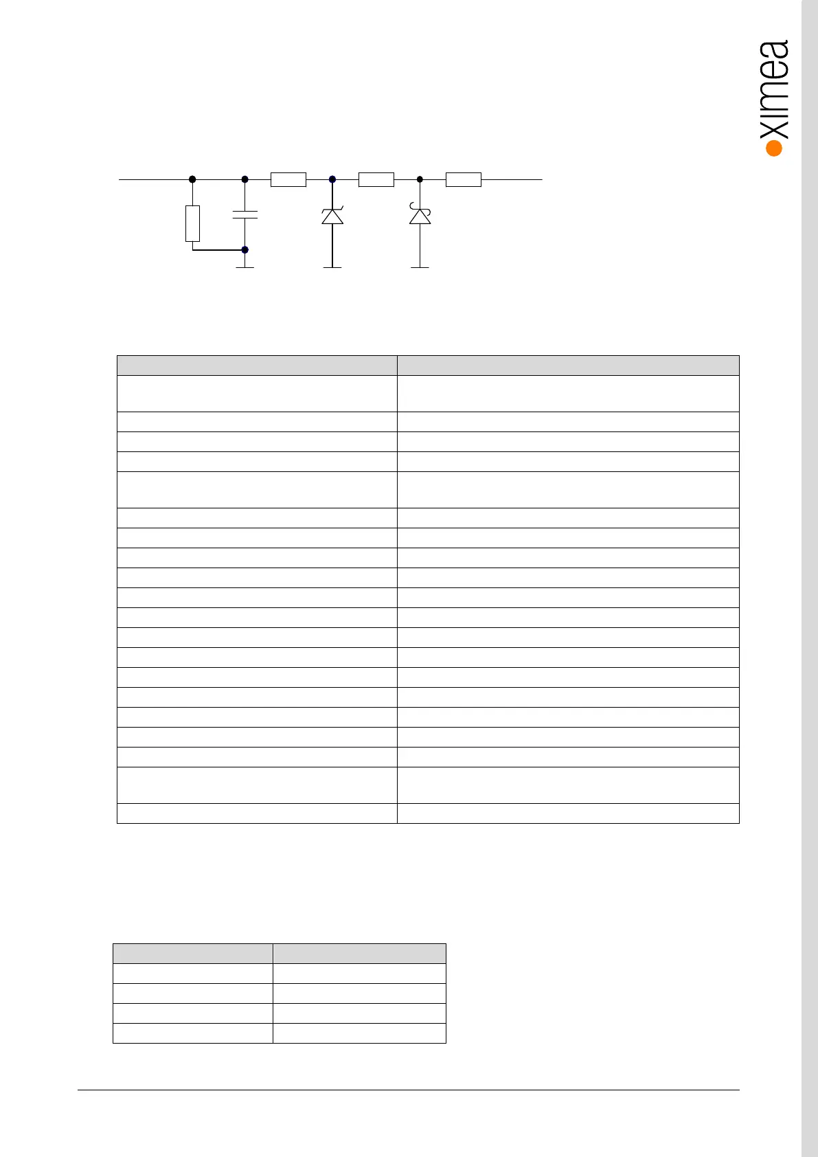
figure 3-56, non isolated input/output, interface schematic
3.10.5.1. Non-isolated Digital Input/Output (INOUT) General info
2, each line can be configured by application separately as input or
output
Effect of incorrect input terminal connection
Reverse voltage polarity protected
Effects when withdrawing/inserting input module
under power
Short-circuit/over-current/reverse voltage
Maximal output sink current
30µA, maximum advised load = 60kΩ
Output delay – rising edge
400ns, Load 100kΩ, threshold 2V
Output delay - falling edge
450ns, Load 100kΩ, threshold 0.5V
Input impedance – minimum
Input level for logical 0
Input level for logical 1
Input delay – rising edge
750ns, V
INPUT
=5V,T
AMBIENT
=25°C
Input delay – falling edge
1
1200ns, V
INPUT
=5V,T
AMBIENT
=25°C
Trigger, get current level; Rising or falling edge are supported for
trigger
Off, On, Exposure active, Frame active; Signal inversion supported
Table 3-40, General info for non-isolated digital in/out trigger lines.
NOTE 1) Because of low input impedance of non-isolated input it is not possible to connect master slave of two cameras
directly. Signal conditioning (buffer, opamp…) is required
3.11. External power supply input (AUX)
0.65A, @5V while acquiring
Over/under voltage protection
* Is model depended. Used values are for MC124MG-SY-TC
FPGA GPIO
100R10k1k0
10p
100k
GNDGNDGND
INOUT