Individual Functions
6-113
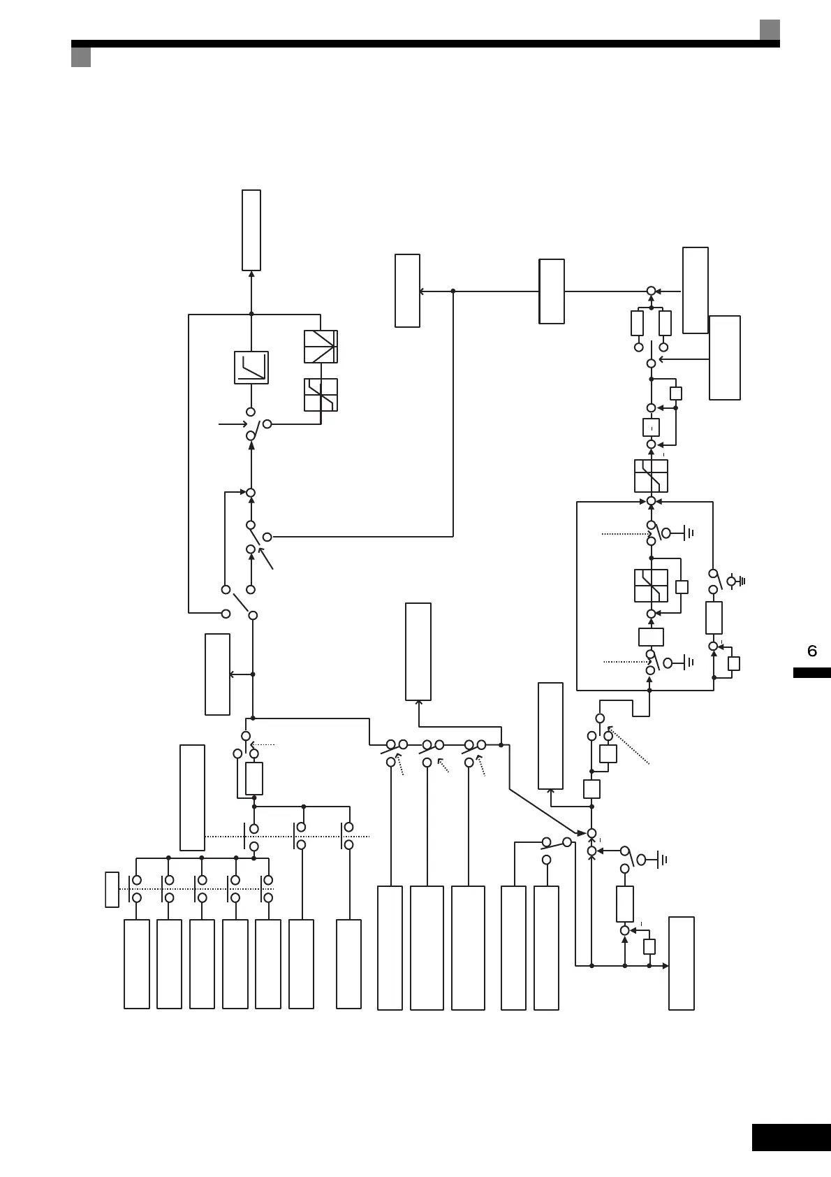
PID Control Block
The following diagram shows the PID control block in the Inverter.
Fig 6.64 PID Control Block
Option Card
Serial Com
Terminal A1
d1-01
d1-02
d1-16
MEMOBUS communications
register 06 H PID target value
Pulse train input
Z
-1
b5-05
Derivative (D)
time
+
+
P
b1-01
0
1
2
3
4
Frequency reference
using multi-step comman
d
PID input volume
(U1-36)
Set PID target value in
multi-function analog inpu
t
Set bit 1 of MEMOBUS
register 0FH to 1
b5-01=2,4
b5-01=1,3
Proportional
gain (P)
b5-02
+
+
b5-17
Pulse input terminal RP
H6-01=2
Pulse input terminal RP
PID feed-back
value (U1-24)
-1
Select multi-function inputs
PID input characteristic
s
0
1
PID SFS Cancel
H6-01=1
Output frequency
(U1-02)
1
T
b5-05
T
1
-1
PID output
gain (b5-10)
Z
-1
Z
-1
Z
-1
Frequency reference
(U1-01)
PID target value
(U1-38)
Integral
(I) time
b5-03
Store integral using
multi-function input
s
Integral (I)
time
b5-04
b5-01=1,3
b5-01=2,4
Derivative
time
Integral rset using
multi-function input
s
PID upper
limit
b5-06
PID Limit
PID first order lag
time constant
b5-08
PID offset
adjustment (b5-07)
Select PID output
characteristics selection
(b5-09)
+
+
+
+
+
+
+
+
+
+
PID output monitor
(U1-37)
b5-01=0
b5-01=3,4
b5-01=1,2
PID ON
PID OFF
Multi-function input PID control cancel
signal is ON. PID is OFF under the
following conditions:
b5-01 = 0
During JOG command inpu
t
b5-11=0
b5-11=1
Enable/disable reverse operation
when PI output is negativ
e
Upper limit
Fmax x109%
Lower limit 0
Upper limit
Fmax x109%
Lower limit
-(Fmaxx109%)
+
+
0
+
1
1
Terminal A2 or A3 PID
target value
Terminal A2 or A3 PID
feedback
H3-05 or
H3-09=B
 Loading...