36 Rockwell Automation Publication 6000-UM002E-EN-P - April 2018
Chapter 2 Drive System Layout
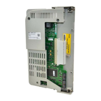
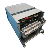
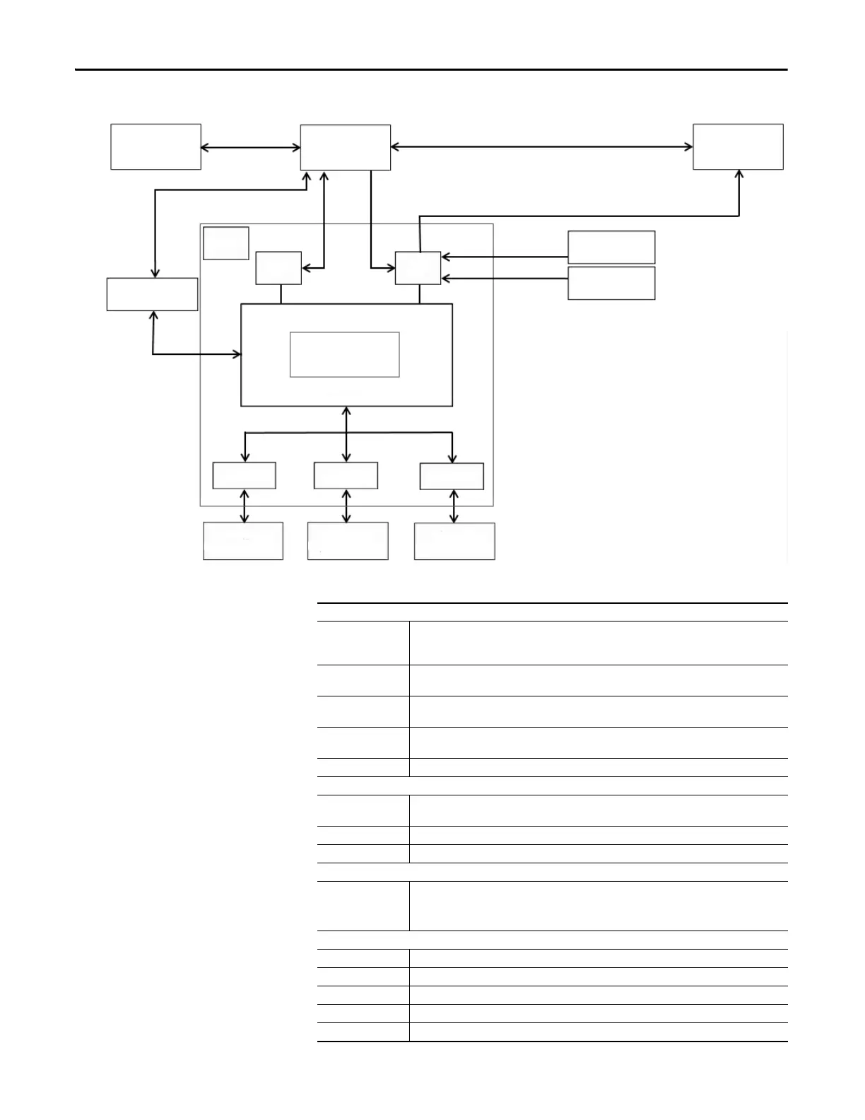
Figure 26 - Control Unit Layout
Table 3 - Control Unit Description
HMI
PWM Board A
DCS
Phase A
Power Modules
Fieldbus
VSB
HECS
PLC
Communication
Board
PWM Board B PWM Board C
Phase C
Power Modules
DT
AT
DB
CPU Board
Phase B
Power Modules
RJ45 Modbus TCP/IP
RS-232
Modbus RTU
Fiber Optic
Board Function
PWM Board A, B, C Output PWM and control signals to Power Modules
Collect and process fault and state information from Power Modules to CPU board
Each phase PWM board can control up to nine power cells
CPU Board Process analog input signals, switch and fault information, control DA and switch signal output,
realize V/F algorithm, set and change parameters in communication with PLC
Analog Signal
Processor Board (AT)
Collect and process analog input signals to CPU Board, output analog signals processed by DT
board
Digital Signal
Processor Board (DT)
Collect and output digital signals, digital to analog conversion function
DB Board Acts as a base board in the Control Unit and interfaces the digital and analog signal cables
Connector
PLC Communication
Interface
Connection between PLC and Control Unit.
Fiber Optic Socket Connection between Power Modules and Control Unit (two per module)
Interface Terminals Connects external inputs and outputs
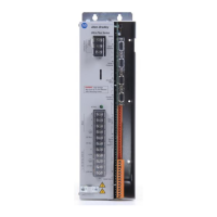
Status Indicators
Phase control board
transceiver indicator
light
B: board healthy indicator
T: transmit data to power module indicator
R: receive data from power module indicator
CPU Board Indicator Lights
RX Receive communication signals from PLC
TX Transmit communication signals to PLC
FPGA FPGA healthy indicator
DSP2 DSP2 healthy indicator
DSP1 DSP1 healthy indicator
 Loading...