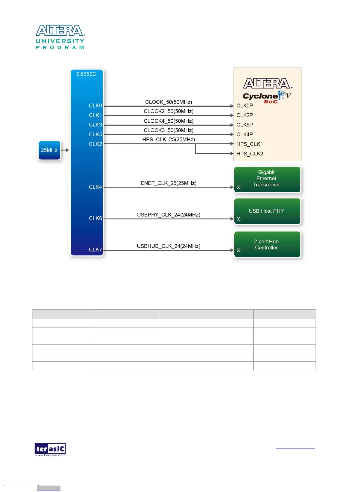
Figure 3-12 Block diagram of the clock distribution on DE1-SoC
Table 3-5 Pin Assignment of Clock Inputs
3
3
.
.
6
6
P
P
e
e
r
r
i
i
p
p
h
h
e
e
r
r
a
a
l
l
s
s
C
C
o
o
n
n
n
n
e
e
c
c
t
t
e
e
d
d
t
t
o
o
t
t
h
h
e
e
F
F
P
P
G
G
A
A
This section describes the interfaces connected to the FPGA. Users can control or monitor different
interfaces with user logic from the FPGA.
Downloaded from Arrow.com.Downloaded from Arrow.com.Downloaded from Arrow.com.Downloaded from Arrow.com.Downloaded from Arrow.com.Downloaded from Arrow.com.Downloaded from Arrow.com.Downloaded from Arrow.com.Downloaded from Arrow.com.Downloaded from Arrow.com.Downloaded from Arrow.com.Downloaded from Arrow.com.Downloaded from Arrow.com.Downloaded from Arrow.com.Downloaded from Arrow.com.Downloaded from Arrow.com.Downloaded from Arrow.com.Downloaded from Arrow.com.Downloaded from Arrow.com.Downloaded from Arrow.com.Downloaded from Arrow.com.Downloaded from Arrow.com.Downloaded from Arrow.com.