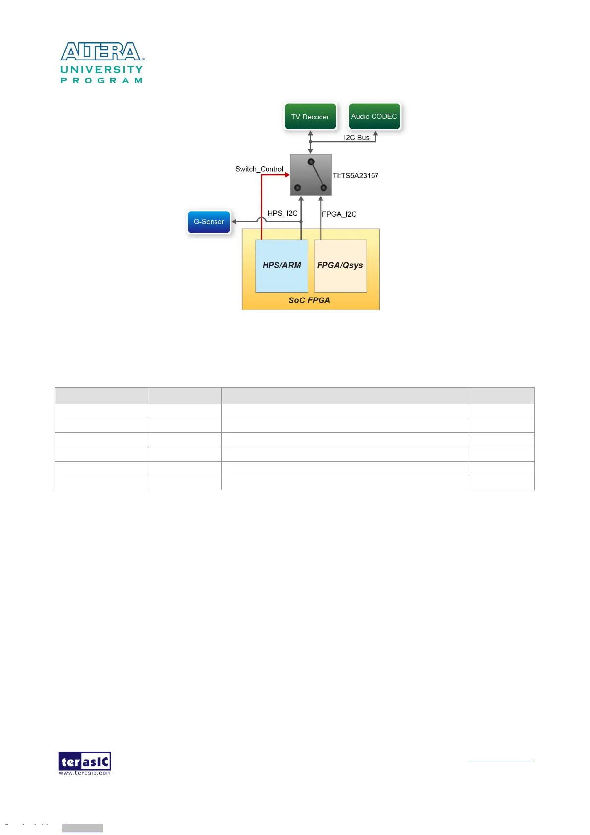
Figure 3-20 Control mechanism for the I2C multiplexer
Table 3-13 Pin Assignment of I2C Bus
I2C Clock of the first HPS I2C concontroller
I2C Data of the first HPS I2C concontroller
I2C Clock of the second HPS I2C concontroller
I2C Data of the second HPS I2C concontroller
3.6.6 VGA
The DE1-SoC board has a 15-pin D-SUB connector populated for VGA output. The VGA
synchronization signals are generated directly from the Cyclone V SoC FPGA, and the Analog
Devices ADV7123 triple 10-bit high-speed video DAC (only the higher 8-bits are used) transforms
signals from digital to analog to represent three fundamental colors (red, green, and blue). It can
support up to SXGA standard (1280*1024) with signals transmitted at 100MHz. Figure 3-21 shows
the signals connected between the FPGA and VGA.
Downloaded from Arrow.com.Downloaded from Arrow.com.Downloaded from Arrow.com.Downloaded from Arrow.com.Downloaded from Arrow.com.Downloaded from Arrow.com.Downloaded from Arrow.com.Downloaded from Arrow.com.Downloaded from Arrow.com.Downloaded from Arrow.com.Downloaded from Arrow.com.Downloaded from Arrow.com.Downloaded from Arrow.com.Downloaded from Arrow.com.Downloaded from Arrow.com.Downloaded from Arrow.com.Downloaded from Arrow.com.Downloaded from Arrow.com.Downloaded from Arrow.com.Downloaded from Arrow.com.Downloaded from Arrow.com.Downloaded from Arrow.com.Downloaded from Arrow.com.Downloaded from Arrow.com.Downloaded from Arrow.com.Downloaded from Arrow.com.Downloaded from Arrow.com.Downloaded from Arrow.com.Downloaded from Arrow.com.Downloaded from Arrow.com.Downloaded from Arrow.com.Downloaded from Arrow.com.Downloaded from Arrow.com.