User Manual California Instruments
CSW Series 9
List of Figures
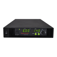
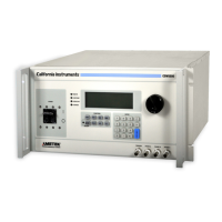
Figure 1-1 California Instruments CSW5550 (With Rack Mount Ears) ................................................................ 12
Figure 2-1: CSW5550 – Typical Current De-Rating Chart for 156v AC Range ................................................... 17
Figure 2-2: CSW5550 – Typical Current De-Rating Chart for 312v AC Range ................................................... 18
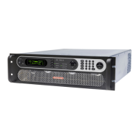
Figure 3-1:CSW5550 ........................................................................................................................................... 28
Figure 3-2:USB Connector pin orientation ........................................................................................................... 34
Figure 3-3: Rear Panel View for the CSW5550) .................................................................................................. 36
Figure 3-4: Output Power Connections for 1 Source and Multi-source Systems ................................................. 39
Figure 3-5: Functional Test Setup ....................................................................................................................... 40
Figure 3-6: Three CSW Sources, 9-phases with Clock/Lock ............................................................................... 41
Figure 3-7: Shuttle Knob ...................................................................................................................................... 44
Figure 3-8: FUNCTION keypad .......................................................................................................................... 45
Figure 3-9: Entering value from decimal keypad ................................................................................................ 46
Figure 3-10: Cursor UP key movement .............................................................................................................. 47
Figure 3-11: Cursor DOWN key movement ........................................................................................................ 47
Figure 3-12: Main Menu 1 screen ....................................................................................................................... 48
Figure 3-13: Menu 1 through 3 ........................................................................................................................... 49
Figure 3-14: PROGRAM Menu ........................................................................................................................... 53
Figure 3-15: MEASUREMENTS Screen, single phase and three phase modes ................................................ 55
Figure 3-16: HARMONICS/TRACE ANALYSIS screen ...................................................................................... 57
Figure 3-17: TRANSIENTS menu ....................................................................................................................... 60
Figure 3-18: VOLTAGE SURGE/SAG SETUP screen ....................................................................................... 61
Figure 3-19: VOLTAGE SWEEP/STEP SETUP screen ..................................................................................... 63
Figure 3-20: FREQUENCY SWEEP/STEP SETUP screen ................................................................................ 65
Figure 3-21: VOLTAGE/FREQUENCY SWEEP/STEP SETUP screen .............................................................. 66
Figure 3-22: START/VIEW TRANSIENT SEQUENCE screen ............................................................................ 67
Figure 3-23: WAVEFORMS menu ...................................................................................................................... 68
Figure 3-24: APPLICATIONS menu ................................................................................................................... 70
Figure 3-25: SETUP REGISTERS menu ............................................................................................................ 71
Figure 3-26: UTILITY menus .............................................................................................................................. 72
Figure 3-27: GPIB/RS232 SETUP menu ............................................................................................................ 75
Figure 3-28: VOLTAGE/CURRENT CONTROL SETUP menu ........................................................................... 76
Figure 3-29: INITIAL SETUP menus ................................................................................................................... 77
Figure 3-30:LIMIT SETUP menu ......................................................................................................................... 78
Figure 3-31: CONFIGURATION SETUP Menus .................................................................................................. 79
Figure 3-32: MEASUREMENT CAL FACTORS menu ........................................................................................ 81
Figure 3-33: OUTPUT CAL FACTORS menu ...................................................................................................... 81
Figure 3-34: Selecting a waveform ...................................................................................................................... 85
Figure 3-35: Selecting waveforms for single phase or all phases ....................................................................... 85
Figure 3-36: Custom waveform creation with GUI program ................................................................................. 86
Figure 3-37: Waveform crest factor affects max. rms voltage ............................................................................. 87
Figure 3-38: Waveform frequency domain view mode ....................................................................................... 88
Figure 3-39: Scrolling through tabular FFT data ................................................................................................. 92
Figure 3-40: Scrolling through bar chart FFT data .............................................................................................. 92
Figure 3-41: Scrolling through acquired waveform data ..................................................................................... 94
Figure 3-42: SET VOLT trigger source acquisition ............................................................................................. 96
Figure 3-43: Positive trigger delay (Post trigger data) ........................................................................................ 97
Figure 3-44: Negative trigger delay (Pre-trigger data) ........................................................................................ 98
Figure 3-45: Pulse Transients ............................................................................................................................. 99
Figure 3-46: List Transients .............................................................................................................................. 100
Figure 3-47: Switching waveforms in a transient list ......................................................................................... 102
Figure 3-48: START/VIEW TRANSIENT SEQUENCE menu ........................................................................... 103
Figure 4-1: Power Source Module Block Diagram ............................................................................................. 106
Figure 4-2: Internal Assembly Locations ........................................................................................................... 108
Figure 5-1: Test Equipment Hook-up for Calibration ......................................................................................... 115
Figure 5-2: Front Panel Assembly Adjustment Location (Top View) .................................................................. 116
Figure 8-1: Application Menu ............................................................................................................................. 124
Figure 8-2: DO160 Main Menu .......................................................................................................................... 124
Figure 8-3: Normal state .................................................................................................................................... 125
Figure 8-4: Voltage Modulation ......................................................................................................................... 127
Figure 8-5: Frequency Modulation ..................................................................................................................... 128
 Loading...