System Control
ARM DDI 0363G Copyright © 2006-2011 ARM Limited. All rights reserved. 4-36
ID073015 Non-Confidential
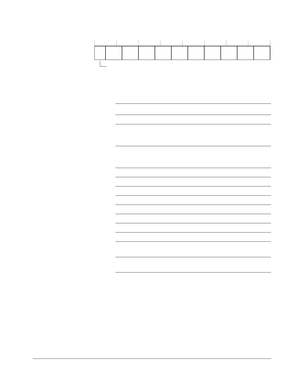
Figure 4-24 shows the CLIDR bit assignments.
Figure 4-24 CLIDR Register bit assignments
Table 4-21 shows the CLIDR bit assignments.
To access the CLIDR, read CP15 with:
MRC p15, 1, <Rd>, c0, c0, 1 ; Read CLIDR
4.3.14 c0, Cache Size Selection Register
The CSSELR characteristics are:
Purpose Holds the value that the processor uses to select the CSSELR to use.
Usage constraints The CSSELR is:
• a read/write register
• accessible in Privileged mode only.
CL 8 CL 7 CL 6 CL 5 CL 4 CL 3 CL 2 CL 1
Reserved
31 30 29 27 26 24 23 21 20 18 17 15 14 12 11 10 8 6 5 3 2 0
LoU LoC
Table 4-21 CLIDR Register bit assignments
Bits Name Function
[31:30] - SBZ
[29:27] LoU Level of Unification:
0b001
= L2, if either cache is implemented
0b000
= L1, if neither instruction nor data cache is implemented.
[26:24] LoC Level of Coherency:
0b001
= L2, if either cache is implemented
0b000
= L1, if neither instruction nor data cache is implemented.
[23:21] CL 8
0b000
= no cache at Cache Level (CL) 8
[20:18] CL 7
0b000
= no cache at CL 7
[17:15] CL 6
0b000
= no cache at CL 6
[14:12] CL 5
0b000
= no cache at CL 5
[11:9] CL 4
0b000
= no cache at CL 4
[8:6] CL 3
0b000
= no cache at CL 3
[5:3] CL 2
0b000
= no cache at CL 2
[2] CL 1 RAZ. Indicates no unified cache at CL1
[1] CL 1
0b000
= no data cache is implemented
0b001
= data cache is implemented.
[0] CL 1
0b000
= no instruction cache is implemented.
0b001
= an instruction cache is implemented.