Description
Technical Manual Version 001 BRUKER BIOSPIN 33 (55)
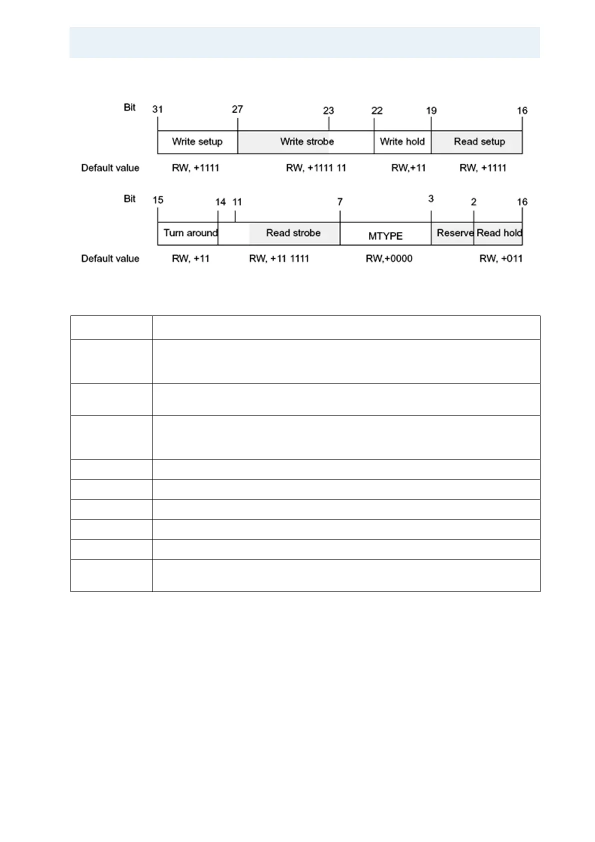
Table 5.20: EMIF Space Control Register Field Description
The MTYPE field identifies the memory type for the corresponding CE space. If
the MTYPE field selects a synchronous memory type (SBSRAM), the remaining
fields of the register have no effect.
The DSP PLL Register
The DSP includes a PLL and a flexible PLL controller peripheral consisting of a
pre-scale (D0) and four dividers (OSCDIV1, D1, D2, D3). The PLL controller is
able to generate different clocks for different parts of the system (DSP core, exter
-
nal memory interface and other peripherals). The picture below illustrates the PLL
and clock generation logic.
Table 5.21: EMIF CE Space Control Register Field Description
Field Description
Read setup
Write setup
Setup width. Number of clock cycles of setup time for address (EA), chip enable (CE),
and byte enables (BE 3..0) before strobe or write strobe falls. For asynchronous read
accesses, this is also the setup time of AOE before ARE falls.
Read strobe
Write strobe
Strobe width. The width of the read strobe (ARE) and write strobe in clock cycles.
Read hold
Write hold
Hold width. Number of clock cycles that address (EA) and byte strobes (BE (3..0)) are
held after read strobe or write strobe rises. For asynchronous read accesses, this is
also the hold time of AOE after ARE rising.
MTYPE Definition for C671x.
MTYPE = 0100: 32–bit wide SBSRAM.
MTYPE = 1010: 8–bit wide SBSRAM.
MTYPE = 1011: 16–bit wide SBSRAM.
TA The turn around time controls the number of ECLKOUT cycles between a read and
write, or between reads, to different CE spaces (asynchronous memory types only).