Description
Technical Manual Version 001 BRUKER BIOSPIN 41 (55)
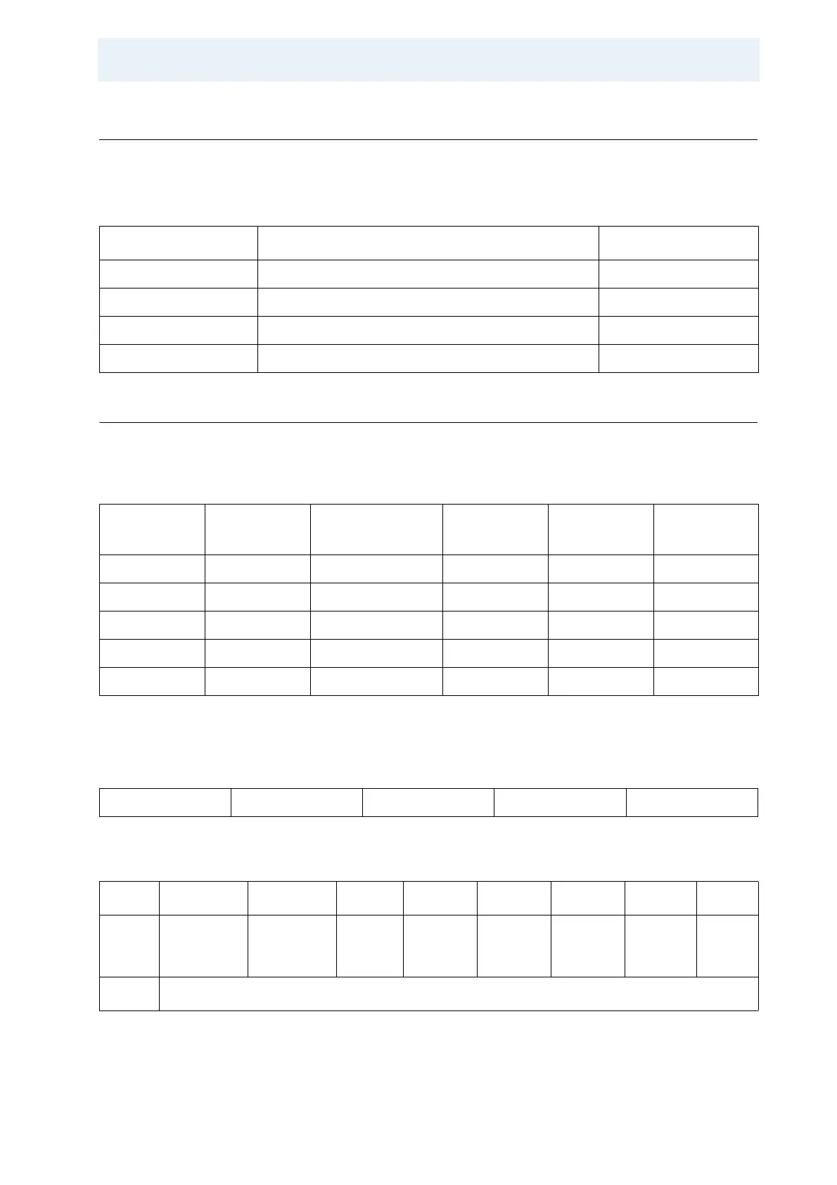
DSP Address Map 5.4.10
Registers at the EMIF Bus 5.4.11
Format of the Control Register
The control word makes the differentiated control of the logic functions possible.
Table 5.34. Memory Region of EMIF Bus
DSP Select Signal DSP Memory Allocation Module
DSP CE 0 0x800000000 - 0x8000FFFF Memory
DSP CD 1 0x90000000 - 0x90000008 Register
DSP CE 2 0xA0000000 Receiver FIFO
DSP CE 3 0xB0000000 Output FIFO
Table 5.35: Address Allocation of the Registers
Register
DSP Select
Signal
DSP Address
PCI Local
Select Signal
Bit Size Used R/W Control
Control CE1 0x9000 0000 9..0 rrrrrw wrrr
Reset CE1 0x9000 0004 4..0 wwwww
Pipeline CE1 0x9000 0008 CS1 15..0 r/w all
Information CE1 0x9000 0020 10..0 rr rrrr rrrr
Debug CE1 0x9000 0024 10..0 rr
CNTR 9000 0000 Control Register R/W 31-0
Table 5.36: Control Register: Bit Fields
Bits
31..9 8..6 5 4 3 2 1 0
Fields
Not
allocated
CALC
Error
Counter
NG
OFF
REC EN SEND
EN
TIME
OUT
CALC INT
Res.
0