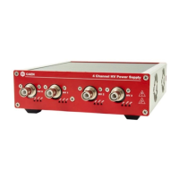
Programmable HV Power Supply
Revision 19
n
CAEN
T o o l s f o r D i sc o v e r y
Fig. 2.7: N1470 ALARM electrical scheme................................................................................................................................ 11
Fig. 2.8: N1470 ALARM TTL configured.................................................................................................................................... 11
Fig. 2.9: N1470 INTERLOCK electrical scheme....................................................................................................................... 11
Fig. 2.10: Remote communication control and RS485 I/O – RS232 IN electrical scheme................................................ 12
Fig. 2.11: HV Channel panel and test point electrical scheme............................................................................................... 13
Fig. 3.1: Welcome screen............................................................................................................................................................. 17
Fig. 3.2: Channel OFF status screen ......................................................................................................................................... 17
Fig. 3.3: Channel ON status screen ........................................................................................................................................... 17
Fig. 3.4: Channel KILL status screen ......................................................................................................................................... 18
Fig. 3.5: Mode settings status screen......................................................................................................................................... 18
Fig. 3.6: Mode settings access screen....................................................................................................................................... 18
Fig. 3.7: Mode settings edit screen............................................................................................................................................. 18
Fig. 3.8: Channel settings edit screen ........................................................................................................................................ 19
Fig. 3.9: Channel VSET select screen ....................................................................................................................................... 19
Fig. 3.10: Channel VSET access screen ................................................................................................................................... 19
Fig. 3.11: Channel VSET digit selection screen ....................................................................................................................... 19
Fig. 3.12: Channel VSET digit access screen........................................................................................................................... 20
Fig. 3.13: Channel VSET digit adjust screen ............................................................................................................................ 20
Fig. 3.14: Channel VSET digit confirm screen .......................................................................................................................... 20
Fig. 3.15: Channel VSET confirm screen .................................................................................................................................. 20
Fig. 3.16: Channel VSET de-select screen ............................................................................................................................... 21
Fig. 3.17: Channel KILL screen................................................................................................................................................... 21
Fig. 3.18: Channel EXIT screen .................................................................................................................................................. 21
Fig. 3.19: Group selection ............................................................................................................................................................ 22
Fig. 3.20: Group active.................................................................................................................................................................. 22
Fig. 3.21: Group VSET access screen....................................................................................................................................... 22
Fig. 3.22: Group VSET digit selection screen ........................................................................................................................... 22
Fig. 3.23: Group Channel VSET digit access screen .............................................................................................................. 23
Fig. 3.24: Group VSET digit adjust screen ................................................................................................................................ 23
Fig. 3.25: Group VSET digit confirm screen.............................................................................................................................. 23
Fig. 3.26: Channel VSET de-select screen ............................................................................................................................... 23
Fig. 3.27: Group EXIT screen ...................................................................................................................................................... 24
Fig. 3.28: USB communication diagram .................................................................................................................................... 25
Fig. 3.29: RS232 communication diagram ................................................................................................................................ 25
Fig. 3.30: RS485 communication diagram ................................................................................................................................ 26
Fig. 3.31: Ethernet communication diagram ............................................................................................................................. 26
Fig. 3.32: RS232 port cable adapter........................................................................................................................................... 27
Fig. 3.33: Main Menu .................................................................................................................................................................... 27
Fig. 3.34: Board Status Menu ...................................................................................................................................................... 28
Fig. 3.35: Channels Menu ............................................................................................................................................................ 28
Fig. 3.36: PC keyboard ................................................................................................................................................................. 28
Fig. 3.37: Channels group setting ............................................................................................................................................... 29
Fig. 3.38: Firmware Upgrade Menu/1......................................................................................................................................... 29
Fig. 3.39: Firmware Upgrade Menu/2......................................................................................................................................... 29
Fig. 3.40: Format EEPROM Menu .............................................................................................................................................. 30
Fig. 3.41: Current offset calibration warning ............................................................................................................................. 30
Fig. 3.42: Current offset calibration VSET selection ................................................................................................................ 30
Fig. 3.43: Current offset calibration confirmation...................................................................................................................... 31
Fig. 4.1: Side cover removal instructions................................................................................................................................... 35
Fig. 4.2: Polarity selection instructions....................................................................................................................................... 36
Fig. 4.3: Dip switch position ......................................................................................................................................................... 37
Fig. 4.4: C21 jumper location ....................................................................................................................................................... 38
Fig. 4.5: Earth configuration connection examples .................................................................................................................. 39
LIST OF TABLES
Table 1.1: Available items ...............................................................................................................................................................5
Table 2.1: Power requirements ......................................................................................................................................................6
Table 2.2: Interlock operation ...................................................................................................................................................... 12
Table 2.3: Mod. N1471 Channel technical specifications ....................................................................................................... 14
Table 3.1: Smileys list ................................................................................................................................................................... 24